
Definition of BJT
A BJT in its full form is written as bipolar junction transistor and we can define it as,
“A bipolar junction transistor is a three-terminal semiconductor device which is made up of two PN junctions within its structure and is mainly used to amplify current”
History of the bipolar junction transistor_ BJT
- Prior to the bipolar junction transistors, vacuum tubes were used in electronic circuits which were highly expensive, those too were available in the form of a triode which was a three terminal device like a transistor back then.
- The vacuum tube triodes remained a hyped-up thing for almost half of a century, but they occupied large space and were less reliable in terms of usage, the other major drawback was the increase in complications related to current, voltage and whatnot just by increasing the number of vacuum triodes in the circuit.
- So when scientists were done with controlling electrons inside a vacuum tube and its unruly behavior, they started devising other ways to run and control circuits.
- Finally, in 1947 the efforts of john Walter and Bardeen a rough two-point contact device was made which was nowhere near to the modern of a bipolar junction transistor but it laid the foundation for the construction of a solid-state transistor when previously everything was vacuum!
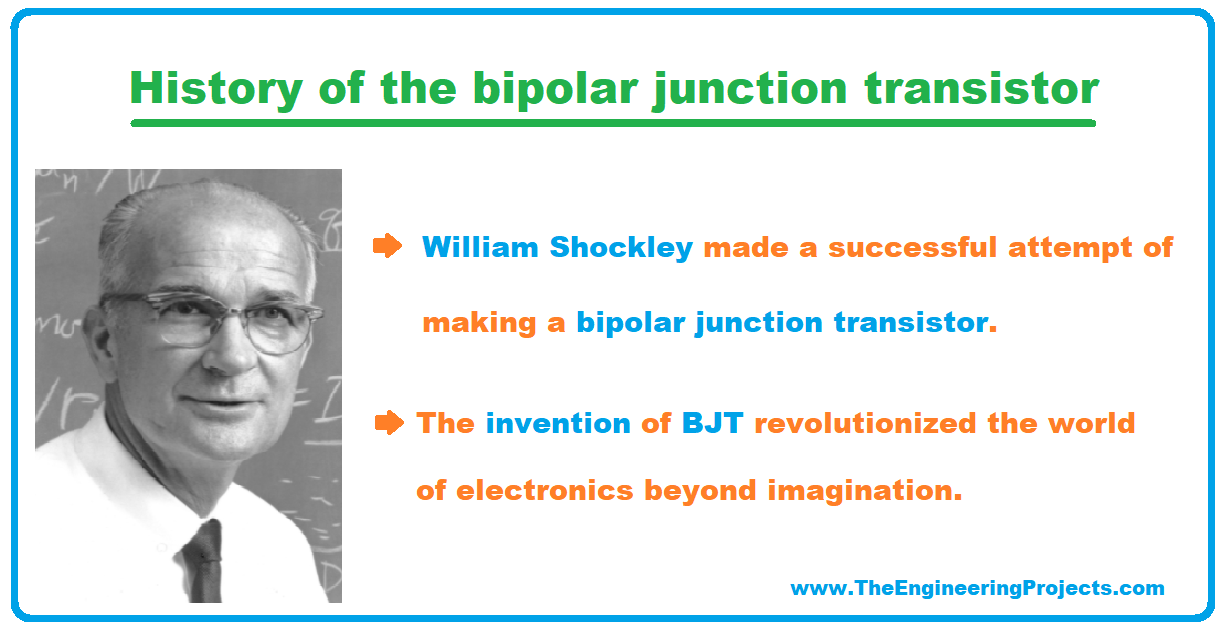
- After this not-so-recognized venture, William Shockley made a successful attempt of making a bipolar junction transistor by pressing together the wafers of semiconductor materials.
- And guess what? William Shockley, John Walter, and Bardeen were awarded with the Noble Prize for their achievements in 1956.
- The invention of bipolar junction transistors revolutionized the world of electronics beyond imagination.
- Until the last decades of the 19th century, bipolar junction transistors were manufactured individually as separate components and individual devices but later on, with the invention of integrated circuits, the world saw another electronic revolution.
Features of BJT
Here are some of the peculiar features of bipolar junction transistors;
- BJT by which we mean bipolar junction transistor is a current-controlled device, you will, later on, get to know how it works. Keep reading!
- As the name indicates BJT is a bipolar device, which means it uses both the electrons and holes as charge carriers to perform its function.
Symbol of BJT
Bipolar junction Transistor shortly known as BJT has the following three components;
- Base
- Emitter
- Collector
- All of the three components are represented in the symbol given below as B, E, and E.
Refer to the diagram given below showing the symbol of NPN and PNP Bipolar Junction Transistors;
- The direction of flow of current is indicated by the direction of Arrowhead.
- Symbols for different types of BJTs differ accordingly, do not confuse yourself when you see two or more slightly different ones!
Working Principle of a Bipolar Junction Transistor
- The working principle of both the NPN and PNP transistor is almost the same, both of them differ in the conduction of current through charge carriers based on the majority and minority of charge carriers.
- The NPN Bipolar junction Transistor has the majority of charge carriers as electrons.
- The PNP Bipolar junction Transistor has the majority of charge carriers as holes.
- The current flow is not the result of majority charge carriers despite their quantity, the current flow is due to minority charge carriers in a bipolar junction transistor that is why they are also named as minority carrier devices.
- The emitter-base junction is always forward biased.
- The collector-base junction represented by CB is always reverse biased.
- The Emitter current is written as IE=IB + IC
- If we consider base current to be very small in actual measurement then we can say that; IE~IC
Types of Bipolar Junction Transistor
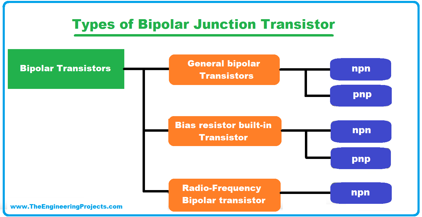
As we already know the basic components of the bipolar junction transistor, we would now discuss its type. Bipolar junction Transistor has the following two types;
- NPN bipolar junction transistor
- PNP bipolar junction transistor
The image given below shows the types of BJT along with their usage for different purposes;
Now we will discuss both of these types in detail.
1. NPN Bipolar Junction Transistor
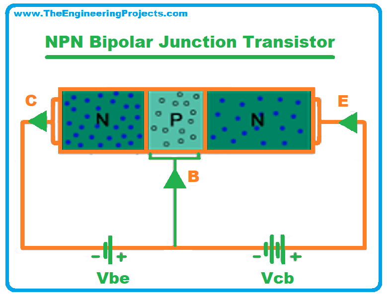
As the name indicates, in an NPN Bipolar junction Transistor a p-type semiconductor is sandwiched between the two n-type semiconductors just as a cheese slice between two sides of a bun.
Refer to the diagram given below for better understanding;
According to the conventional rules when the current moves into a certain component of the transistor it is labeled as positive meanwhile when it leaves the component it is labeled as negative.
As we already know, NPN transistor consists of two PN junctions, made by fusing the two n semiconductors with one p-type semiconductor. The n-type emitter region is heavily doped because of the fact that it has to pass on charge carriers to the base.
The base is not heavily doped and is very thin as compared to the emitter and collector, imagine the size of cheese slice as compared to the buns! It transfers charge carriers to the corresponding collector.
The collector of the NPN transistor is moderately doped and as the name indicates, it collects the charge carriers from the base.
Working of NPN Bipolar Junction Transistor
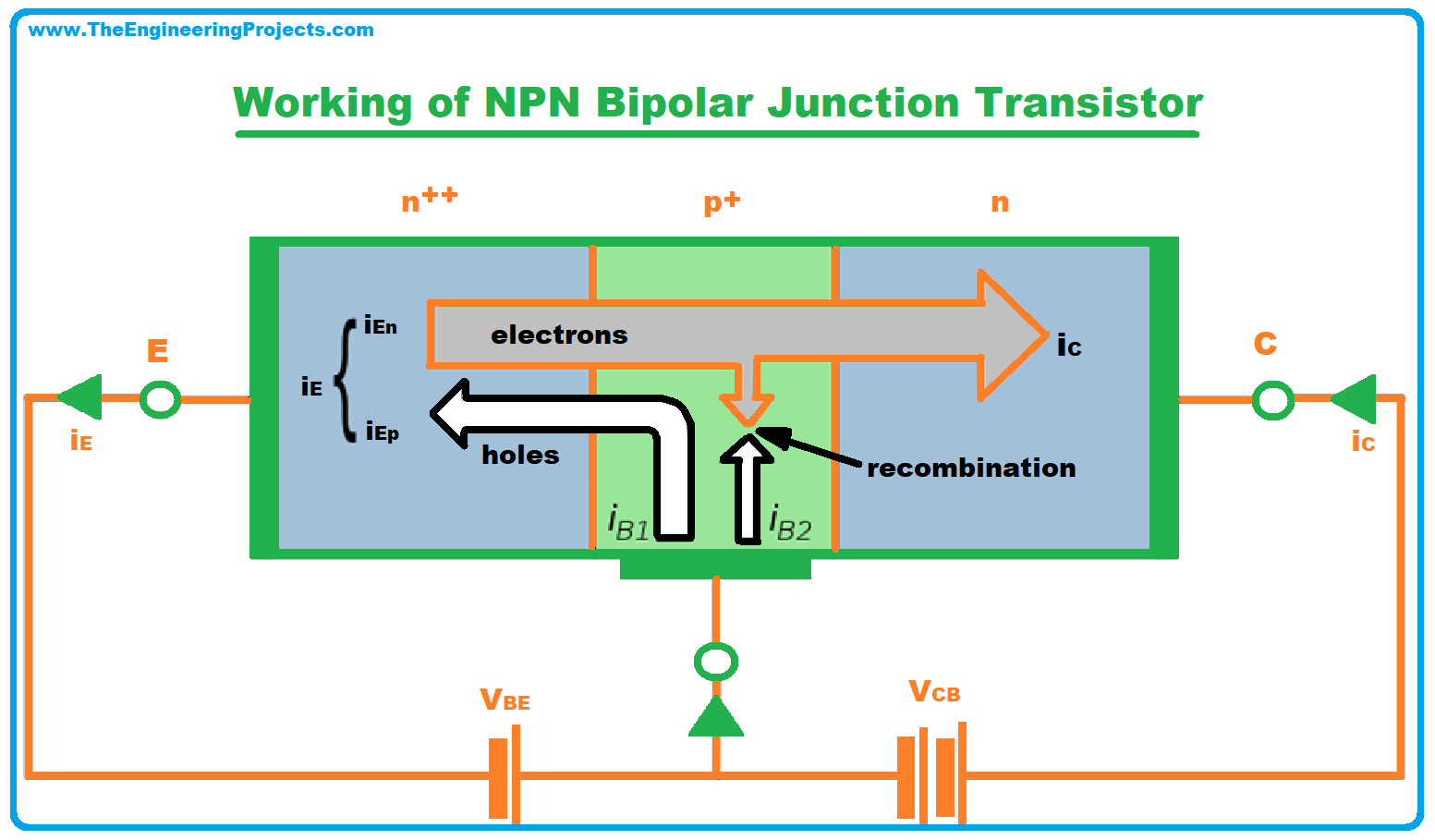
- Consider the following circuit diagram in order to understand how an NPN Bipolar junction Transistor works.
- As already told, the NPN Bipolar Junction Transistor has two PN junctions, so for forward biasing we connect the base-emitter junction with the power supply VBE.
- The collector-base junction represented by CE Junction is reverse biased by applying the voltage VCB.
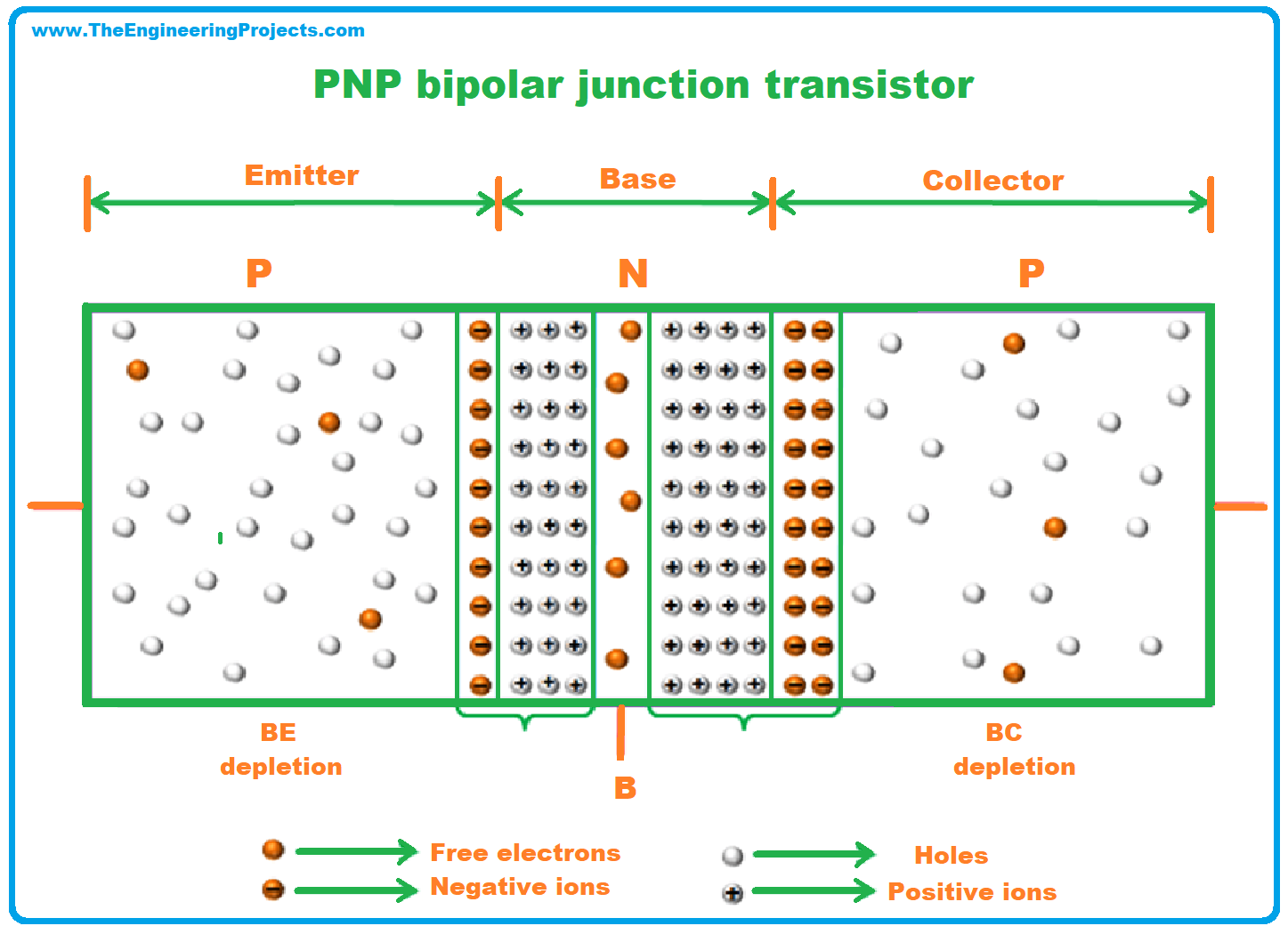
- The depletion region of the two PN junctions varies in size, do you remember what a depletion region is? In simple words depletion region opposes the flow of current, it acts like a barrier or a block to current flow and is the area where mobile electrons are not present. Have a look at the diagram given below,
- You must be thinking about why the emitter-base region has a smaller depletion region, meanwhile, the collector-emitter junction has a wider one? Let me solve it for you, It is due to the reason that the base-emitter region is forward biased!
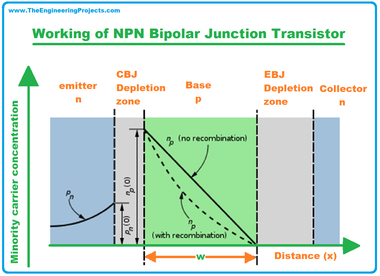
- NPN type Bipolar junction Transistor has a majority of electrons , when the emitter-base junction is forward biased, the electrons start flowing towards the base which is lightly doped, only a few of the electrons would combine with the base holes and the rest of them would then travel to the collector. The current is due to minority charge carriers as we discussed earlier.
- The current flowing through the emitter-base junction is the emitter current IB, meanwhile, the current flowing through the base is called base current and is represented by IB.
- Base current IB is very limited as compared to the other types of current present in the circuit.
- The remaining electrons which missed the recombination pass through the collector-base region to the collector which produces the collector current IC.
- The emitter current is written as; IE = IB+ IC
PNP bipolar junction transistor
- PNP bipolar junction transistor is made up of two layers of p type semiconductor which sandwiches the n type semiconductor layer in between.
- The entrance for the current is emitter terminal in PNP Bipolar Junction Transistor.
- The emitter base junction represented by EB is forward biased in this case.
- On the parallel lines collector base junction represented by CB is reverse biased.
- The emitter current IE is positive meanwhile base current IB and collector current IC is negative.
- When we talk about the voltage, VEB the emitter base voltage is positive meanwhile VCB and VCE are negative.
- NPN and PNP bipolar junction transistors work on the same principle, the only difference they have is of the majority and minority charge carriers. Can you figure out the current flow in a PNP transistor from the image given below?
I-V Characteristics of Bipolar Junction Transistor
To study the input characteristics, output characteristics, and common current characteristics we need to understand the different configurations of bipolar junction transistors.
There are three types of configurations for bipolar junction transistors, let’s list all the three;
- Common Base configuration
- Common emitter configuration
- Common collector configuration
- First things first, do you have any idea about the characteristics of a Bipolar Junction Transistor, or what are they? And how we determine them? Putting it straight, The I-V characteristics of Bipolar Junction Transistor is simply the graphical manifestation of the current and voltage of a transistor.
- To study the characteristics cover of the bipolar junction transistor, we will go through the different modes of a Bipolar Junction Transistor which you would be seeing in the curves.
Working Modes of a Bipolar Junction Transistor
There are three dominant regions in which a bipolar junction transistor works;
- Active region
- Saturated region
- Cut off region
Active Region of a Bipolar Junction Transistor
- In The active region of a bipolar junction transistor in which the collector base region is forward biased meanwhile the emitter base junction is reverse biased.
- In the active region of a bipolar junction transistor, the transistor works as an amplifier.
Saturated Region of a Bipolar Junction Transistor
In the saturated region the Bipolar Junction Transistor passes a saturated current after reaching a maximal value of threshold voltage. In the saturated region, our bipolar junction transistor works as a switch, an ON switch, and the collector current is fairly equal to the emitter current.
Cut Off Region of a Bipolar Junction Transistor
As the name indicates there is no collector current in the circuit in this region. The transistor is off and the collector is in a reverse-biased state.
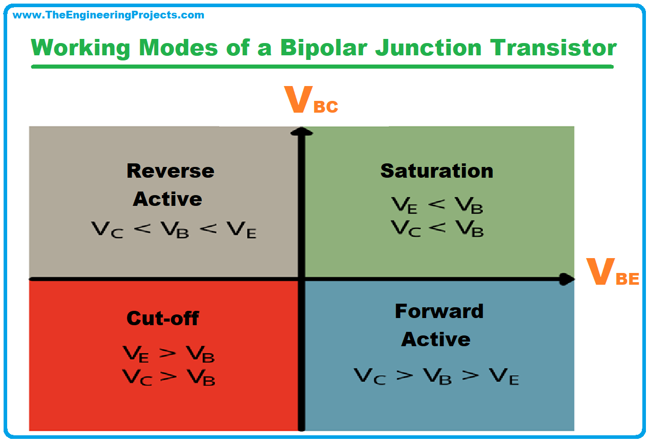
The image given below reflects the overall voltage story of BJT in different regions;
As we are done with the regions and modes in which our Bipolar Junction Transistor works, let us discuss different configurations and their input and output characteristics
Common Base Configuration of a Bipolar Junction Transistor
In the common-base configuration, the base terminal of Bipolar Junction Transistor is connected within the input and output terminals of the transistor.
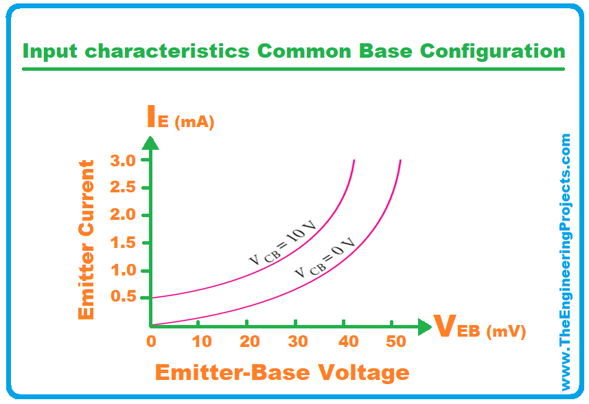
Input characteristics Common Base Configuration of a Bipolar Junction Transistor
- The input characteristics are plotted between the emitter current IE and the emitter-base voltage VEB for the varying values of collector-base voltage VCB.
- We can clearly observe the trend from the graph that, The Emitter base junction is forward biased so the emitter current IE increases with the increasing values of VEB as the collector base Voltage VCB increases.
Output characteristics Common Base Configuration of a Bipolar Junction Transistor
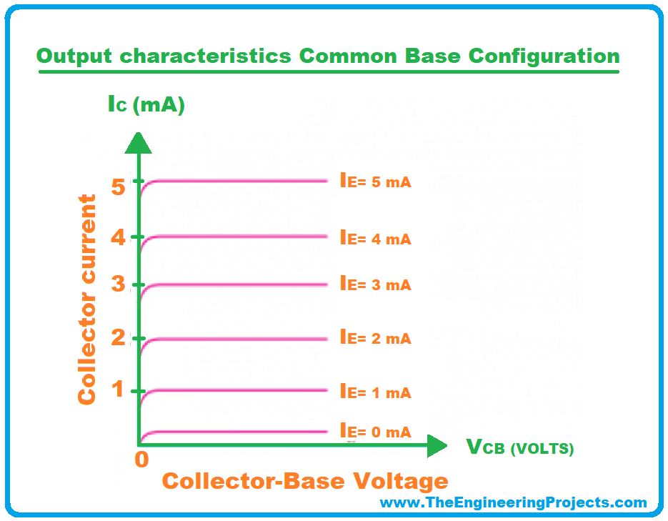
- The output characteristics of Common Base Configuration of a Bipolar Junction Transistor are plotted between the output voltage VCB and output current IC, follow the graph given below for better understanding;
- Change in the emitter current IE results in the changing values of collector current IC.
- The Emitter current IE and Emitter Base Voltage VEB are positive because the region is forward biased.
- You can observe the active region in the graph, the phase in which the transistor operates at its maximal potential.
Common emitter configuration of a bipolar junction transistor
In the common-emitter configuration of a bipolar junction transistor, the emitter terminal is connected between both the input and output terminals, the thing you already know! Don’t you?
Input characteristics Common emitter configuration of a bipolar junction transistor
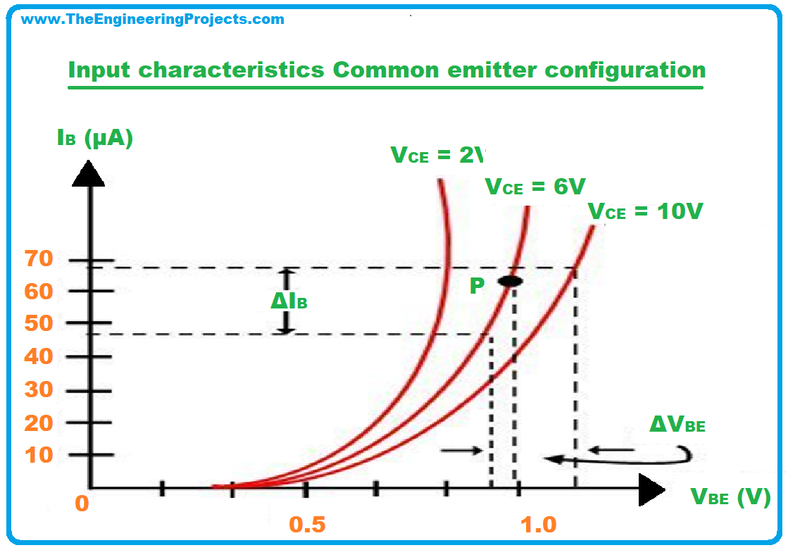
- The graph for the Common emitter configuration of a bipolar junction transistor is plotted between the base current IB and the Base emitter voltage of VBE, for the increasing values of Collector-Emitter voltage, as you can see in the graph plotted below;
- We can clearly observe from the plotted graph, that the value of base current increases with the increasing value of base-emitter voltage.
Output characteristics Common emitter configuration of a bipolar junction transistor
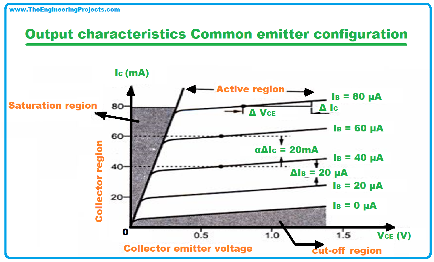
- For the common emitter configuration, the output characteristics are plotted between the collector current IC with the varying values of collector-emitter voltage VCE.
- The graph represents the working of the bipolar junction transistor in three regions namely saturated region, active region, cut off region.
- The active region is the region in which the current increases with the voltage but it has not reached its maximal value.
- The saturated region represents the saturated current when the voltage has reached its maximal value. Can you spot all the mentioned regions in the graph given above?
- In the cut-off region, the emitter region is reverse biased with a minimal amount of current.
Early effect in Bipolar Junction Transistor
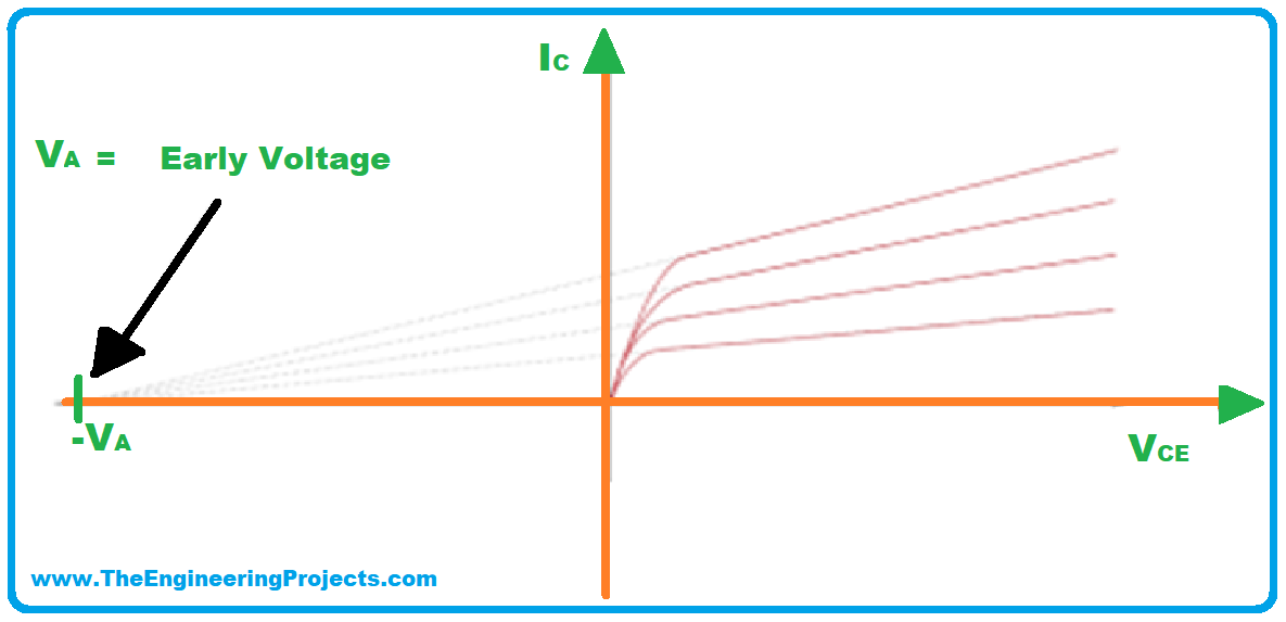
- Here is another important term to be discussed when we are discussing the output characteristics of the bipolar junction transistor which is known as The Early Effect of a bipolar junction transistor, this phenomenon holds an important place when we talk about the I-V characteristics of a bipolar junction transistor. So, without any further delay let’s see what is Early Effect in a BJT?
- As some of you might have presumed Early effect is one of the earlier manifestations of the collector current or anything like this, let me burst your bubble, it is definitely not true! Early effect in the Bipolar Junction Transistor is named after the scientist James M Early.
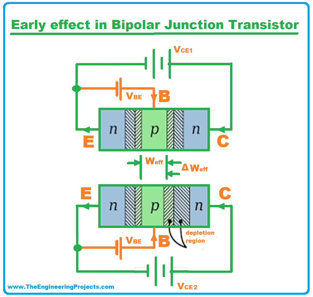
- Early effect in the bipolar junction transistor is the change in the effective width of the base region by applying the collector-base voltage VCB.
- The circuit diagram given below represents the early effect in a bipolar junction transistor;
- It causes the increase in reverse bias condition of the collector-base junction or in simple words it amplifies the reverse biasing of the collector-base junction causing a considerable decrease in the width of the Base region of the Bipolar junction Transistor.
- The early effect is fairly important in the output characteristics of common emitter and common collector configuration.
- Due to the Early Effect in bipolar junction transistor, the Collector Current represented by IC increases by the increasing the Collector-Emitter Voltage VCE.
- Consider the following graph for better understanding;
Common Collector Configuration of a Bipolar Junction Transistor
You might go through the following names of common collector configuration, we all have nick names and alternate names, and same goes for this configuration;
- Grounded collector configuration
- Voltage follower circuit
- Emitter follower circuit
- In Common Collector Configuration of a Bipolar Junction Transistor, The collector terminal is kept common within the input and output terminal of the circuit, as we are at the end of our discussion, can you tell which is the input terminal and which one is the output terminal?
- The input terminal is the place where the input signal for the base is given meanwhile the output terminal is the point where the Output signal is obtained between the collector and the emitter.
- An important thing to note is that the common collector configuration has very high input impedance.
Input characteristics Common Collector Configuration of a Bipolar Junction Transistor
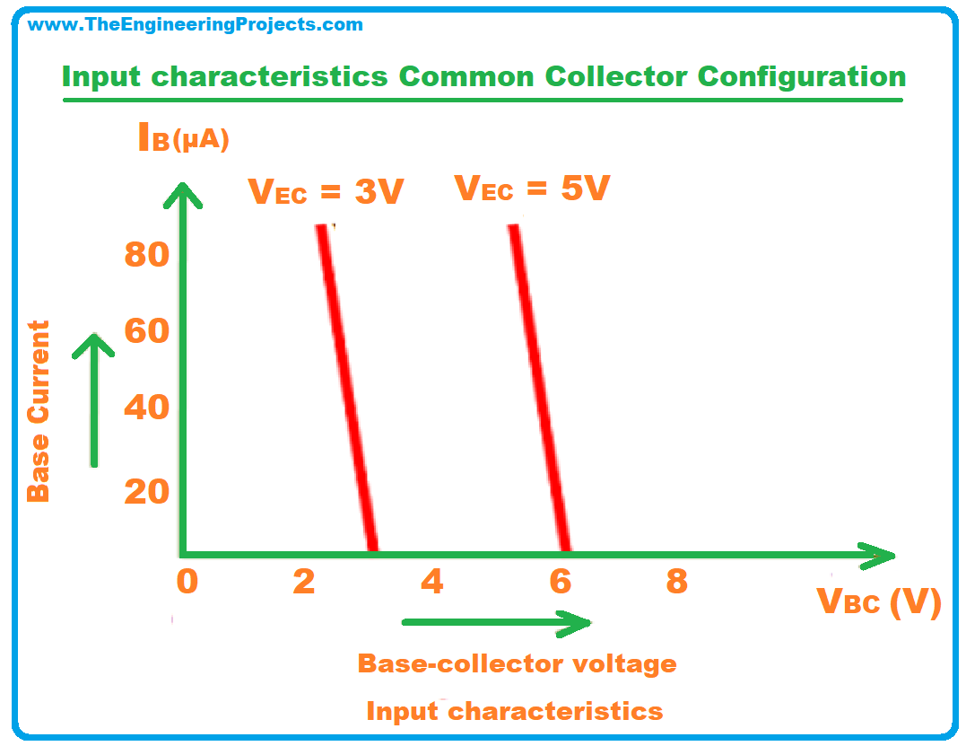
- The input characteristics for Common Collector Configuration of a Bipolar Junction Transistor are plotted between the base current IB and Base collector voltage VBC. Refer to the following graph for better understanding,
- The base current IB is presented on the y axis meanwhile the collector-base voltage VCB is presented on the x-axis.
- The output voltage VBC increases with the increasing value of IB, you can follow the graph for better understanding.
Output characteristics of Common Collector Configuration of a Bipolar Junction Transistor
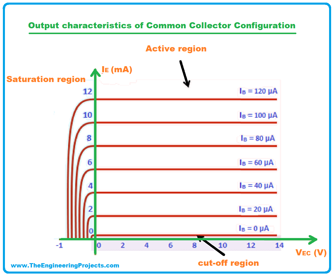
- The output characteristics of the common collector configuration are plotted between the emitter current IE and emitter-collector voltage VCE. Follow the graph for better understanding;
- The output for the voltage VCE is plotted for different values from zero to the maximal range.
- You can observe different regions for the output values, such as the Saturation region, Active region, and cut-off region of the graph, I hope by now you have a clear idea what these regions represent. These are the same corresponding values as we studied earlier in the emitter-collector configuration.
Comparison of bipolar junction transistor with other transistors
As we have been discussing the transistors lately, Let us compare bipolar junction transistors with other types of available transistors such as Field-effect transistor FET and MOSFET, metal oxide semiconductor Field-effect transistor. The following section would help you find clear difference between the BJT and FET.
BJT vs FET/JFET
- First things first, both of these transistors belong to two different families of the transistor.
- The bipolar junction transistor as the name clearly indicates is bipolar and JFET/FET is unipolar. If you don’t have any idea about the unipolar and bipolar transistors, let me tell you, they are named after the conduction process which involves only one type of charge carriers taking the name of unipolar transistors and the one requiring both types of the charge carriers electrons as well as holes, they are named bipolar transistors.
- Bipolar Junction Transistor is a current-controlled device meanwhile FET is a voltage-controlled device.
- Bipolar junction transistors are a bit noisy than FETs.
- Bipolar junction transistors have higher input impedance than the Field-Effect Transistors.
- Bipolar junction transistors have lesser thermal stability than the FETs
- There are three functional components of a bipolar junction transistor named as base, emitter, and collector, meanwhile, FET has different components named as the base, source and drain.
- Bipolar junction transistors are larger in size than the JFETs.
- Bipolar junction transistors is less expensive than the Field effect transistor.
As you might already know that Junction Field Effect Transistors are a type of Field Effect Transistors so I haven’t made a separate heading for the comparison of BJT first with FETs overall and then individually with JFET and MOSFET.
Comparison is the thief of joy so this upcoming section about the comparisons of BJTs would be the last one for the Bipolar Junction Transistors, Let’s begin;
BJT vs MOSFET
Let us now compare bipolar junction transistors with MOSFET;
- BJT stands for bipolar junction Transistor meanwhile MOSFET stands for Metal Oxide Field-Effect Transistors.
- A bipolar junction Transistor is a current controlled device meanwhile MOSFET is a Voltage Controlled Device.
- A bipolar junction Transistor has three components named as emitter-collector and a base, meanwhile, a MOSFET has four components being the body, source, drain, and gate.
- The output of a Bipolar junction Transistor can be controlled by controlling Base current meanwhile output of a MOSFET can be controlled by controlling Gate voltage.
- Bipolar junction Transistor has a negative temperature coefficient meanwhile MOSFET has a positive temperature coefficient.
- Both Bipolar junction transistors and MOSFET are used for switching but the bipolar junction Transistor has a low switching frequency meanwhile MOSFET high switching frequency.
- Bipolar junction transistor is a bipolar device meanwhile MOSFET is a unipolar device.
- Bipolar junction Transistor has a high input impedance meanwhile MOSFET has a low input impedance.
- Bipolar junction Transistors are a bit noisy than MOSFETs.
- Bipolar junction Transistors are used in low current applications meanwhile MOSFETs are used in high power applications.
- MOSFETs are preferred for industrial use as compared to bipolar junction transistors because of their higher efficiency.
In case you want a detailed overview on the MOSFET, you can read our detailed article on this topic including definition, types, working and applications.
Applications of the Bipolar Junction Transistor
As we are done with our discussion on the basics and types of bipolar junction transistors let us discuss some of their applications.
We already know the bipolar junction transistors are simple and cheaper to manufacture with lesser efficiency than other modern transistors such as MOSFET, there are still some areas where only BJTs are used because as they say old is gold! Let’s move to the last segment of our discussion
BJTs have countless uses, but here is a brief list for you to go through before we study the detailed applications of Bipolar Junction Transistors through and through;
- BJT can be used in clipping circuits, for a detailed outlook on this you can read our article on transistors.
- Bipolar Junction Transistors are used for signal demodulation.
- We use BJT for amplifying current due to its current gain characteristics.
- High-frequency applications such as radio frequency also involve Bipolar Junction Transistors.
- Bipolar Junction Transistors are used for discrete circuit designs because of their easy availability and low-cost manufacturing.
- Bipolar Junction Transistors are frequently used in analog circuits.
Now it’s time to have a detailed discussion on the applications of a bipolar junction transistor;
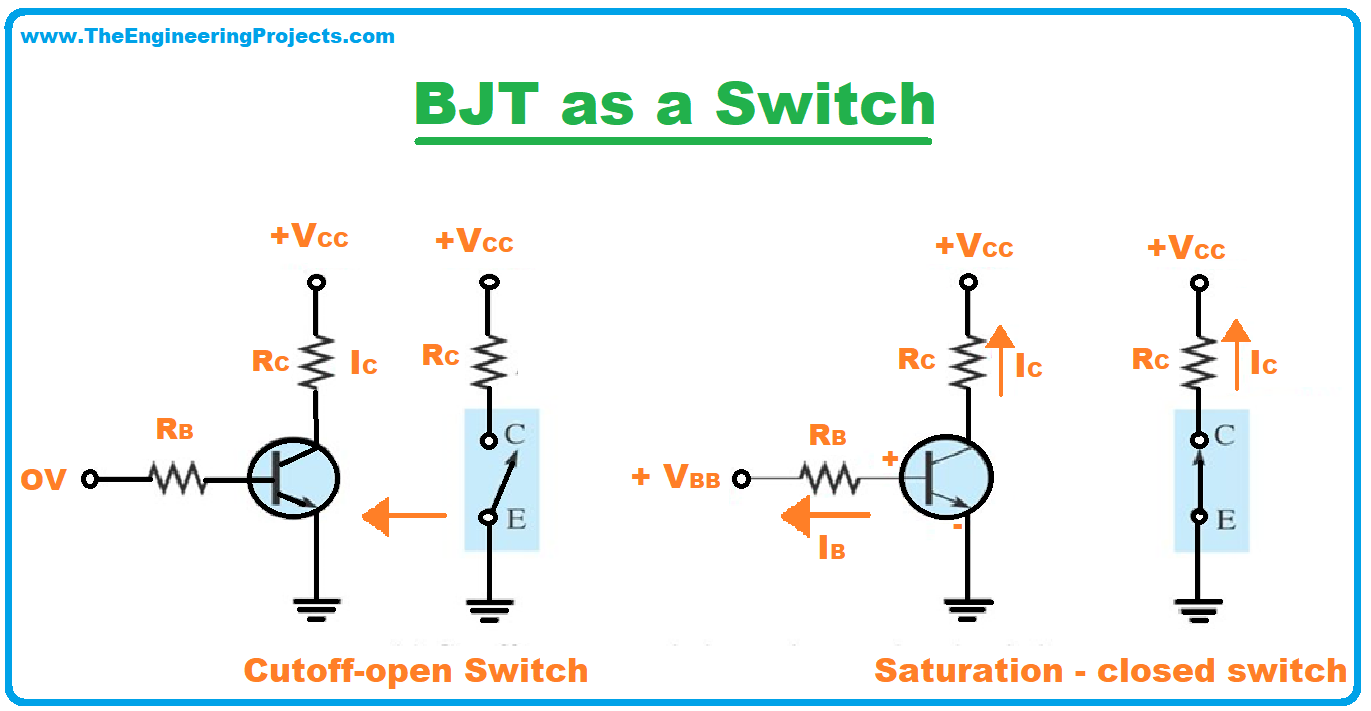
1. BJT as a Switch
- You can easily guess how a BJT can work as a switch as we have already discussed its working in detail. Let us go through a brief breakdown of the process;
- When we have to use a Bipolar Junction Transistor as a switch, we need to keep our circuit on the toes, i.e. we have to constantly alter the current between the saturation phase and the cut off phase of a bipolar junction transistor. Can you recall both the phases? In case you can’t scroll up and read it again.
- In the cut off phase there is reverse biasing of collector base junction and we do not get any current.
- Meanwhile in the saturation phase of the Bipolar Junction Transistor it is working on its maximal potential.
- When the Bipolar Junction Transistor is operational in its Saturation region, there is no voltage drop across the circuit and it is carrying maximal current according to its definite capacity, in this condition we take it as a closed switch.
- On the parallel lines, in the cut off region, there is no conduction of current due to reverse biasing so we can say that our Bipolar Junction Transistor is working as an open switch.
- Now you know, how our Bipolar Junction Transistor also known as BJT works as a switch.
2. Bipolar Junction Transistor as Amplifiers
- If you can recall the characteristics of the bipolar junction transistor you might remember that a BJT acts as an amplifier when it is operated in its saturated region.
- The current gain of the bipolar junction transistors depends upon the alpha and beta characteristics of the transistor.
- Due to a huge current gain, the bipolar junction transistor is used in amplifiers in different configurations we have already discussed in detail, can you recall any of them? No worries, I’m listing the three of them again;
- Common-base configuration
- Common-emitter configuration
- Common-collector configuration
3. Bipolar Junction Transistors in Logic Gates
- Who has not been through the world of logic gates if he or she is somehow related to the world of electronics! I was always in a love-hate relationship with the logic gates.
Emitter Coupled Logic
- Bipolar junction transistors are a significant part of ECL, emitter-coupled logic.
- The ECLs are never ever operated in saturated mode, they have a high input impedance and low output impedance.
- The current keeps on rolling between the ECL pair hence each gate constantly keeps on drawing current, can you think of any of the disadvantages it may cause? Let me solve it for you, The ECL dissipates more energy than the other families of transistors.
- The Emitter Coupled logic is also named as;
- Current mode logic CML
- Current switch emitter follower logic CSEMFL
- Current Mode logic CML
Fusion of MOSFET and BJT
- The other new hyped-up thing is the fusion of MOSFET and BJT making a BiCMOS, a bipolar CMOS which reaps the benefits of both, the bipolar junction transistor and MOSFET.
- In case you are trying to figure out the meaning of that C in BiCMOS, please don’t open a new tab, I’ll let you know, it stands for Complementary metal-oxide-semiconductor, thank me later!
4. Bipolar junction transistors as logarithmic converter
- The changes in the junctions of the BJT are logarithmic as we already know that the voltage of our base-emitter changes with the change in the algorithm of our current in the collector-emitter and base-emitter current during different biasing modes.
- So due to this specialty and predictability in the nature of bipolar junction transistors, we can easily make a BJT to calculate logarithms and anti-logarithms in any circuit.
- You must be thinking that we can render a diode for this purpose as well, why are we not using a diode instead? The answer lies in the high circuit flexibility and stability of a Bipolar Junction transistor, which a diode can’t provide.
5. Bipolar junction transistors in Temperature Sensors
- In our previous section, we discussed that the temperature coefficient for the Bipolar Junction transistors is small, so due to this property they can be used as temperature sensors.
- Now you must be thinking how we can do that practically, there is a simple method to measure the temperature.
- The base-emitter junction of a BJT has a very stable and predictable current transfer function which depends on temperature, which is why Bipolar Junction transistors are used in Temperature sensors.
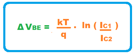
- Following relationships exists between the current and voltage of the two junctions at different temperatures;
In the above-mentioned equation;
- K is the Boltzmann constant
- T is the temperature in Calvin
- VBE is the Base emitter current
- IC1 and IC2 are the output current at the same temperature on two different junctions.
So friends, this last segment on the applications of BJT concludes our discussion on Bipolar Junction Transistor. I presume you have learned something new from the article, I know some of the portions are a bit difficult to grasp as well especially if you are reading it for the very first time, but don’t worry it is not humanly possible to understand everything at once, give it another chance even if it is the bipolar junction transistor or anything else in your life, a second turn never hurts anyone! I’ll see you soon with another discussion, Have a good day ahead!
The post BJT: Definition, Symbol, Working, Characteristics, Types & Applications appeared first on The Engineering Projects.


No comments:
Post a Comment