Showing posts with label ELE Times. Show all posts

Wednesday, 22 December 2021

Rohde & Schwarz Collaborates with Broadcom on Test Solution | ELE Times

Rohde & Schwarz, today announced the availability of test solutions for the Broadcom 6GHz Wi-Fi 6E chipsets, the industry’s first to operate in the 6 GHz band. In collaboration with Broadcom Inc., Rohde & Schwarz has successfully verified the new R&S CMP180 next-generation wireless device test platform, which is especially suitable for R&D as well as production. OEMs and ODMs of wireless equipment, who integrate Broadcom Wi-Fi 6E chipsets, now have access to the right test solution for R&D, quality control, and production prototyping.

The IEEE 802.11ax amendment (Wi-Fi 6/6E), operating in the 2.4 GHz, 5 GHz and 6 GHz bands, intends to improve WLAN system efficiency, especially the throughput per station in dense signal environments and outdoor environments. With up to 1.2 GHz of Wi-Fi spectrum available for unlicensed use in the 6-GHz band, Wi-Fi 6E can access up to seven 160-MHz channels to support various bandwidth-driven use cases.

These technologies pose challenges for test and measurement equipment. For example, the 1024QAM modulation requires signal generation capabilities which transmit reference signals with very low distortion over a bandwidth of up to 160 MHz and the required analysis bandwidth. The R&S CMP180 has been qualified for characterizing Broadcom 6 GHz Wi-Fi chipsets at the RF level for tests such as error vector magnitude (EVM), timing measurements and spectrum emission compliance. Rohde & Schwarz also provides a Wireless Manufacturing software for Broadcom 6 GHz Wi-Fi chipsets and service solutions to OEMs and ODMs.

Christoph Pointner, Senior Vice President Mobile Radio Testers at Rohde & Schwarz, says: “We are happy to provide tailored test solutions that help Broadcom’s customers bring the newest Wi-Fi technology to the market. The joint efforts with Broadcom for Wi-Fi 6E also provide a solid foundation to enhance our test solution for next-generation Wi-Fi 7, which will leverage on the 6 GHz band to deliver higher performance and throughput.”

Gabriel Desjardins, Director of Product Marketing in the Wireless Communications & Connectivity Division at Broadcom Inc., says: “We continue to collaborate with Rohde & Schwarz in developing 6 GHz Wi-Fi test systems. The availability of these systems has enabled our customers and partners to accelerate deployment of 6GHz Wi-Fi.”

The R&S CMP180 radio communication tester is a future-proof, non-signaling testing solution for wireless devices in research and development, validation and production. Together with advanced frequency, bandwidth and RF capabilities, it enables testing of new wireless technologies such as Wi-Fi 6E, Wi-Fi 7 and many more. Additionally, the doubled number of analyzers (2xVSA), generators (2xVSG) and RF ports (2×8) enable simultaneous measurements of technologies and devices in a VSA/VSG single-box tester.

For more information, visit www.rohde-schwarz.com

The post Rohde & Schwarz Collaborates with Broadcom on Test Solution appeared first on ELE Times.

Sunday, 19 December 2021

element14 Launches Arduino UNO Anniversary Design Challenge | ELE Times

element14, an Avnet Community, is celebrating 16 years of the Arduino UNO by offering members the chance to win a limited edition Arduino Uno Gold Mini, one of the best and most robust boards to get started with electronics and coding.

It is a unique black and gold board with almost the same specifications as the iconic Arduino Uno, a board synonymous with the Arduino itself. It comes with the same processor, pinouts and performance that made the UNO so popular but there are a couple of cool tweaks – the board is a quarter of the size of the original footprint, measuring 34.2mm x 26.7mm x 8mm, and USB port has been updated to USB-C allowing for a smaller form factor.

The Arduino UNO has and continues to give many members of the element14 Community the foundation they need to contribute to the electronics design world. In honor of this popular board’s anniversary, the five best-completed projects using an Arduino board will win a limited edition Arduino Gold Mini.  The members can also win a swag bag with an Arduino board by simply submitting their ‘Build a Present’ project proposals that uses an Arduino board. Other prizes for completed projects include shopping carts, tool kit bundles, and gifts to give to other members for their projects.

“The Arduino UNO has inspired some of the most fun and creative projects on the community,” said Dianne Kibbey, Global Head of Community and Social Media for the element14 Community. “We’re thrilled to be able to offer a limited-edition Arduino UNO Mini to members of our community to help further inspire imaginative and unexpected designs.”

The Arduino UNO anniversary competition is open now through January 14 2022. Participants can submit a “Build a Present” project proposal, sharing the electronics gift they could build using an Arduino UNO, for the chance to be one of five winners to win a limited-edition Arduino Mini Gold Uno. Winners will be announced on February 4, 2022.

Participants looking for inspiration for their Arduino UNO Anniversary design challenge submissions can review recent creative projects developed on the community featuring the Arduino UNO, including:

  • A Music Box
  • A Cardboard Drum Kit
  • A Robot with Wheels
  • A Marshmallow Roaster
  • A Ham Radio Transceiver

For more information, visit www.element14.com 

The post element14 Launches Arduino UNO Anniversary Design Challenge appeared first on ELE Times.

ROHM’s New Compact Surface Mount 45W Output AC/DC Converter ICs | ELE Times

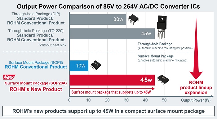
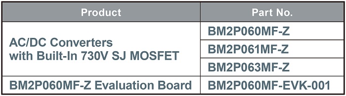
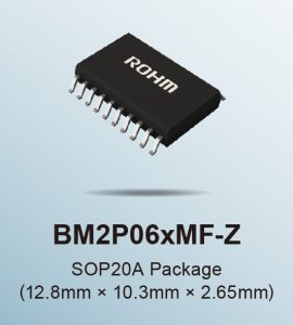
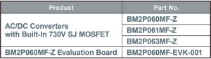
ROHM developed the AC/DC fly-back converter ICs with an integrated 730V breakdown MOSFET in the BM2P06xMF-Z series (BM2P060MF-Z, BM2P061MF-Z, and BM2P063MF-Z). These devices are ideal for auxiliary power supply and Switch Mode Power Supply (SMPS) solutions for industrial drives as well as home appliances – including air conditioners, white goods, and factory automation equipment. These fly-back ICs require no additional heatsinks and no discharge resistors and capacitors. It helps designers to shorten design time, simplify the circuitry, reduce cost and increase reliability by offering integrated solutions.
In recent years, AC/DC converters for home and industrial use must not only support 85V-264V AC to accommodate different AC voltages around the world but also comply with international standards such as Energy Star for energy savings and the IEC 62368 safety standard. It is also important for AC/DC converter ICs to be surface mount to reduce factory mounting costs. However, as high heat/high loss DMOSFETs and planar MOSFETs are still widely used in AC/DC converter ICs, until now it has been difficult to provide tens of watts of output power in a surface mount package.
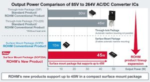
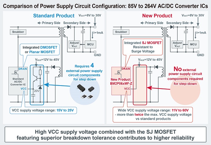
To solve these issues, ROHM developed new compact surface mount high power 45W models BM2P06xMF-Z. They are equipped with an original low-loss SJ (Super Junction) MOSFET together with optimized PWM control circuitry – facilitating the development of 85V to 264V AC/DC converters. Adopting a surface mount package supports automatic board mounting (which was previously difficult to do in the past). Meanwhile, the implemented functions ensure compliance with the IEC62368 safety standard, even when the discharge resistor (a source of loss during standby) is removed. Additionally, original low standby power control technology is applied – resulting in extremely low standby power consumption. Supply voltages up to 60V (VCC) are also supported – eliminating the need for an external step-down power supply circuit.

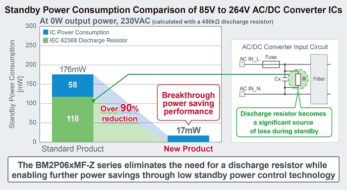
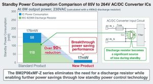
Compared to general products with equivalent performance, automatic mounting contributes to lower factory mounting costs. Moreover, ROHM is able to reduce standby power by over 90% along with the number of power supply circuit components by four, contributing to greater power savings and higher reliability in applications.

Going forward, ROHM will continue to deliver greater system energy savings and optimization by not only developing a wide range of power semiconductors and advanced analog ICs, but also by providing optimal solutions for each application.

Key Features

  1. 45W class surface mount package significantly reduces factory mounting costs

These latest products integrate a low loss (low ON resistance) 730V SJ MOSFET along with both startup and optimized control circuits in a compact high heat dissipation surface mount package (SOP20A). In addition to compatibility with input voltages from 85V to 264V AC, the surface mount package supports high output power up to 45W (24V × 1.875A=45W), which has been difficult to achieve in the past, while significantly reducing mounting costs by enabling automatic mounting not possible with general through-hole types.

  1. Reduces standby power consumption by 90% or more over standard products

The BM2P06xMF-Z series utilizes a control circuit (X capacitor discharge function) that leverages ROHM’s high voltage process and analog design technoloAC/DCgies to meet the safety requirements of the IEC 62368 standard even without a discharge resistor (which is a source of loss but was previously essential). At the same time, original low standby power control technology (which provides optimal control of the switching frequency of power semiconductor and current flowing through the isolation transformer) further reduces IC power consumption during application standby, resulting in a system standby power consumption of just 17mW (at 0W output, 230VAC) – reducing standby power consumption by more than 90% vs general products.
Also included is a noise reduction mode that suppresses noise from the isolation transformer components. This mode can be turned OFF to decrease standby power or be turned ON and adjusted if there is a concern about isolated transformer component noise or a need to minimize the workload for countermeasures.

3. Decreases the number of power supply circuit components by four along with the risk of power semiconductor failure, contributing to higher reliability
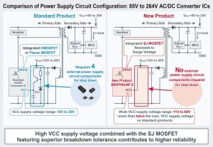
AC/DC

These new products support operation over a wide VCC voltage range from 11V to 60V. The maximum power supply voltage of 60V is twice that of standard products, providing superior reliability against external noise and surge voltages. At the same time, it is possible to reduce the number of external step-down power supply circuit components that are typically required by four, while the internal SJ MOSFET which is resistant to surge voltage [featuring an avalanche (breakdown) tolerance more than 30x higher than DMOSFET and planar MOSFETs used in general products] contributes to higher system reliability by reducing the risk of power semiconductor failure.

Application Examples

◇ Consumer electronics such as air conditioners, appliances, monitors, and hair dryers

◇ Industrial equipment including inverters, AC servos, routers, and office automation devices

Suitable for AC/DC converters up to 45W output in consumer and industrial applications

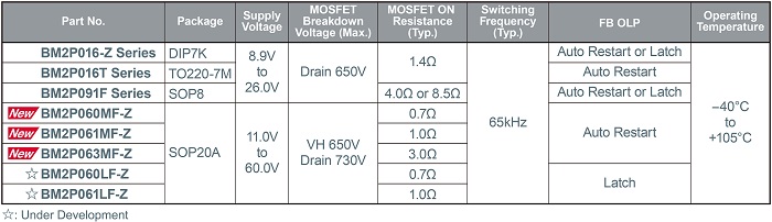
New Product-Related AC/DC Converter IC Lineup

AC/DC

Pricing: $2.13/unit (samples, excluding tax)

Availability: Now (samples), January 2022 (mass production)

Online Sales Information

Sales Launch Date: September 2021

Online Distributors: Digi-Key, Mouser, and Farnell

Product:
AC/DC

Terminology

MOSFET (Metal-Oxide-Semiconductor Field-Effect Transistor), SJ MOSFET (Super Junction MOSFET), DMOSFET (Double-diffused MOSFET), Planar MOSFET

A type of transistor, MOSFETs can be divided by device structure into DMOSFET, planar, and SJ topologies. When produced on Si substrates, DMOSFETs and planar MOSFETs can be made more cheaply than SJ MOSFETs, but SJ MOSFETs can provide superior breakdown voltage and output current along with lower loss when handling large power.

AC/DC Converter

A type of power supply that converts voltage from AC (Alternating Current) to DC (Direct Current).

IEC 62368

A product safety standard for IT and AV equipment. Developed based on the concept of Hazard Based Safety Engineering (HBSE), it defines the scale and manner in which an energy source can be transmitted to cause pain or injury to the human body.

Energy Star

A system of energy efficiency standards for consumer products created by the US Environmental Protection Agency (EPA) and the US Department of Energy (DOE) in 1992. This system is operated in other countries through an international collaborative program covering a wide range of products, including home appliances and IT.

X Capacitor

A capacitor is used for noise reduction in the input circuit of AC power supplies (AC/DC converters). Immediately after unplugging from the outlet, the capacitor remains charged with voltage, so touching the plugin in this state may cause the electricity to be discharged, resulting in electric shock.

For more information, visit www.rohm.com 

The post ROHM’s New Compact Surface Mount 45W Output AC/DC Converter ICs appeared first on ELE Times.

Change of Date: Embedded World Exhibition&Conference 2022 to be held in June | ELE Times

To meet multiple requests from registered exhibitors and enable all participants to plan with the maximum possible confidence, the embedded world Exhibition&Conference 2022 has been rescheduled: In close consultation with exhibitors, the decision has been taken to postpone the exhibition and accompanying conferences until 21-23 June 2022.

  • Early decision to accommodate industry expectations
  • Exhibitors and participants at embedded world Conference and electronic displays Conference can plan with confidence

Exhibitions and congresses have been held again at the Exhibition Centre Nuremberg since September 2021 subject to a robust hygiene concept, and exhibitors and visitors have responded extremely positively and with a sense of responsibility. At the same time, NürnbergMesse is paying attention to the individual needs of its customers and participating sectors. This has led to different decisions for different events. Current developments in the Covid-19 pandemic are causing uncertainty for many exhibitors at embedded world, for example. Benedikt Weyerer, Executive Director embedded world, comments: “By deciding at an early stage to defer embedded world 2022 until summer, we are meeting the wishes of many exhibitors and enabling them to plan with confidence. We are very grateful for the many constructive conversations with industry representatives, which provided significant encouragement for this decision. Together with the exhibitors, we are looking forward to seeing the international embedded community again in Nuremberg from 21 to 23 June next year!”

The embedded world Conference will be held in parallel with the exhibition. As usual, this highly regarded conference will focus on the latest topics of interest, and participants can look forward to seeing mega-trends on the agenda. Professor Axel Sikora, Chairman of the embedded world Conference, is looking forward to the 20th event in the series: “The embedded world Conference 2022 will once again highlight the current state of research and development. This will be another opportunity for us to combine wide-ranging themes relating to the development of complex, comprehensive systems with special themes of current interest such as RISC‑V and solutions to problems in times when supplies of chips are tight, and also long-term megatrends such as artificial intelligence (AI), open-source solutions and secure connectivity. The embedded world Conference brings together the leading thinkers in this area, who are already developing innovations for the future.”

In the area of display technology, the electronic displays Conference brings researchers, developers and decision-makers together. “Micro-LEDs and OLEDs are a hot topic for 2022, for example,” reports the Chair of the Conference Committee, Professor Karlheinz Blankenbach from the University of Pforzheim.

Save the Date

The next embedded world will take place at the Exhibition Centre Nuremberg from 21 to 23 June 2022.

The post Change of Date: Embedded World Exhibition&Conference 2022 to be held in June appeared first on ELE Times.

Enhancing the Performance of GaN SG HEMTs: The New EiceDRIVER 1EDN71x6G HS 200 V Single-Channel Gate Driver Family | ELE Times

Minimized R&D efforts and costs as well as robust and highly efficient operation of medium-voltage gallium-nitride (GaN) switches are key requirements for modern power electronics systems. In accordance with its strategically-designed GaN product portfolio to continuously strengthen full system solutions, Infineon Technologies AG introduces the EiceDRIVER 1EDN71x6G HS 200V single-channel gate driver ICs family. The new product family is designed to enhance the performance of CoolGaN Schottky Gate (SG) HEMTs but is also compatible with other GaN HEMTs and Silicon MOSFETs. The gate drivers aim at a wide range of applications including DC-DC converters, motor drives, telecom, server, robots, drones, power tools, and class D audio amplifiers.

1EDN71x6G variants come with selectable pull-up and pull-down driving strengths, enabling waveform and switching speed optimization without the need for gate resistors. This leads to a smaller power stage layout with fewer BOM components. The strongest/fastest driving variant (1EDN7116G) is suitable for half-bridge configurations with significant paralleling. The weakest/slowest driving variant (1EDN7146G) can be employed for some dv/dt-limited applications like motor drives or very small-die GaN (high-RDS(on), low Qg) HEMTs. Each variant also has a different blanking time, proportional to the minimum recommended dead-time, the minimum pulse width, and the propagation delay.

The truly differential logic input (TDI) feature eliminates the risk of false triggering due to ground bounce in low-side applications and enables 1EDN71x6G to address even high-side applications. Additionally, all variants feature an active Miller clamp with an exceptionally strong pull-down to avoid induced turn-on. This offers extra robustness against glitching in the gate driving loop, especially when driving transistors with a high Miller ratio.

Furthermore, 1EDN71x6G offers active bootstrap clamping to avoid overcharging the bootstrap capacitor during dead-time. This provides bootstrap supply voltage regulation that protects the high-side transistor’s gate without requiring an additional regulation circuit. An optional programmable charge pump with adjustable negative turn-off supply is also provided for additional Miller-induced turn-on immunity when needed, e.g. when PCB layout cannot be fully optimized.

For more information, visit www.infineon.com

The post Enhancing the Performance of GaN SG HEMTs: The New EiceDRIVER 1EDN71x6G HS 200 V Single-Channel Gate Driver Family appeared first on ELE Times.

Exclusive Offers on T&M Equipment Now Available from element14 | ELE Times

element14, an Avnet Company and global distributor of electronic components, products and solutions, has launched an end-of-year promotion to offer exclusive discounts on test and measurement equipment from leading global suppliers including Tektronix and Keithley Instruments, Keysight Technologies, Rohde & Schwarz, Fluke, NI and many more. These special offers are available from element14 until 31st December.

Test and measurement equipment supports the design process, allowing engineers to check their designs are performing as required. element14 is working in partnership with some of its key supplier partners to offer an expert selection of oscilloscopes, handheld test equipment, software and more, to ensure engineers can access the latest solutions at competitive prices to meet their needs.

Customers can take advantage of up to 55% off featured products, including:

  • 15% off the Tektronix TBS1000C digital oscilloscope
  • Up to 55% off a range of Rohde & Schwarz products including power supplies and power analysers, oscilloscopes, RF and microwave signal generators, spectrum analyser kits.
  • 10% off GW Instek’s PSW30-36 programmable power supply
  • 30% off NI’s LabVIEW digital courses which cover how to develop data acquisition (DAQ), instrument control, data-logging and measurement analysis applications in the LabVIEW programming environment. The course also explains dataflow programming and common LabVIEW development techniques.

element14 offers a full range of market-leading test, tools and production supplies from stock to support electronic design and test, with no minimum order value and an educational discount programme. Customers have free access to online resources, data sheets, applications notes, videos and webinars with excellent customer and technical support available 24/5 in local language.

For more information, visit www.element14.com 

The post Exclusive Offers on T&M Equipment Now Available from element14 appeared first on ELE Times.

Thursday, 18 November 2021

STMicroelectronics Boosts Flexibility and Speed with Enhancements to ST25DV Dual-Interface NFC Tags | ELE Times

STMicroelectronics has increased the I2C-interface performance in the latest generation of its ST25DV -I2C dynamic NFC-tag ICs, which let the host system access the tag’s on-chip EEPROM more quickly and easily.

Writing to the EEPROM on the new ST25DV-I2C tags, via the I2C interface, is now as fast as standard EEPROM and allows flexible use of the tag to reduce system bill-of-materials costs. Also, designers can now configure the tag’s I2C address to ensure coexistence with other devices on the bus.

As a Type 5 NFC tag certified by the NFC Forum, the ST25DV-I2C supports contactless interaction with 13.56MHz RFID readers and NFC phones, permitting common use cases such as tap-to-connect pairing with NFC Data Exchange Format (NDEF) messages. The new tags also extend wireless capabilities, including support for arbitration that allows more convenient access to data written into the EEPROM through the RF interface.

With its extra performance and flexibility, this latest evolution of the ST25DV-I2C boosts productivity and efficiency in industrial applications such as smart metering, asset tracking, and logistics, and brings superior user experiences to medical equipment, smart-home devices and lighting, smart retail labels, and consumer products. ST’s ST25DV tags can fulfil multiple use cases throughout a product’s lifetime, including configuration and product tracking, user features, field maintenance, and end-of-life management.

The new tags retain their robustness and convenient features including support for Fast Transfer Mode and energy harvesting. ST’s innovative Fast Transfer Mode leverages a 256-Byte buffer to accelerate handling large files such as a host-system firmware update. Integrated circuitry to control energy harvesting provides an unregulated output voltage for powering external components in battery-less applications.

ST’s ST25DV dynamic tags are compliant with the NFC Forum Type-5 specification and contain up to 64Kbits of EEPROM, with features including configurable password protection for user memory and an interrupt pin that can be programmed to respond to various events detected at the RF interface.

The evolved ST25DV-I2C tags are available in SO-8, TSSOP-8, and chip-scale packages including 8-lead UFDFPN, 12-lead UFDFPN, and WLCSP-10. The ST25DV-I2C Series Dynamic Tags are now available for free sampling and purchase on our eStore and the prices start from $0.33 for orders of 1,000 pieces in the SO8 package with 4Kbit EEPROM.

For further information please visit https://www.st.com/st25dv-i2c.

The post STMicroelectronics Boosts Flexibility and Speed with Enhancements to ST25DV Dual-Interface NFC Tags appeared first on ELE Times.

New Rohde & Schwarz Radome Tester Delivers Fast, Accurate and Cost-Effective Production Line Measurements | ELE Times

The new R&S QAR50 from Rohde & Schwarz is the ideal solution for measuring radomes and bumpers in production. The tester’s innovative design ensures short measurement times and accurate, reproducible results with a very attractive price/performance ratio. A highly modular software concept allows the R&S QAR50 to be adapted to individual requirements.

Advanced driver assistance functions require automotive radar sensors. For design reasons, these are usually installed behind bumpers or emblems. As experience with the R&S QAR has shown, radome quality is strongly dependent on the transmission loss, reflectivity and homogeneity of the components under test.

The R&S QAR and R&S QAR50 use microwave imaging, which has numerous advantages compared to conventional, unfocused single-point measurements. Particularly in production, simple and reliable operation and short cycle times are crucial. The user-friendly interface of the R&S QAR50 simplifies measurements in the automotive radar frequency band – even for users without detailed RF knowledge. Numerous optimizations allow measurement times well below five seconds, significantly reducing cycle times in production.

The imaging method also provides information on whether the components under test are properly positioned. While single-point measurements only display the frequency response of reflectivity for a specific point, the tester also displays the spatial distribution of reflectivity. Tracking the point of maximum reflection provides information on component positioning. Since this method allows the transmit and receive antennas to be far apart without affecting the measurement results, the R&S QAR50 offers significantly more space for clamping and unclamping the components to be measured. The clearance height of around 100 cm between the antenna clusters minimizes the mechanical effort required to position the components. This eliminates the need for robot positioners and carriages, and the enclosures required for occupational safety can be significantly smaller.

The modular software concept allows the R&S QAR50 to be cost-effectively adapted to the specific requirements of the vehicle manufacturer. Depending on the software configuration, complete limit tests for transmission loss, transmission phase, homogeneity and reflectivity can be performed in the frequency and spatial domains. All software options can also be purchased later, ensuring the long-term usability of the R&S QAR50 in end-of-line (EOL) deployment.

The R&S QAR50 for measuring radomes and bumpers in production is now available from Rohde & Schwarz.

The post New Rohde & Schwarz Radome Tester Delivers Fast, Accurate and Cost-Effective Production Line Measurements appeared first on ELE Times.

LANXESS’ High Performance Materials Business Unit to Become Legally Independent | ELE Times

Specialty chemicals company LANXESS will transfer its High-Performance Materials (HPM) business unit to an independent legal corporate structure.

HPM is one of the leading suppliers of high-performance plastics. The materials are used primarily in the automotive, electrical and electronics industries. Electromobility in particular is a promising field of application for the LANXESS plastics, which are used predominantly for car bodies, battery housings and charging infrastructure.

“The global market for new forms of mobility is developing very dynamically and is strategically rearranging itself – creating many innovative alliances and partnerships. In order to get the most out of the growth opportunities in this market and to be able to act flexibly, we will create a separate legal structure for the business unit,” said Hubert Fink, member of the Board of Management of LANXESS AG. LANXESS will begin implementation in the first half of 2022.

The portfolio of the HPM business unit includes the engineering plastics polyamide and polybutylene terephthalate, as well as thermoplastic fiber composites. The business unit is characterized by the high backward integration of its production processes.

The business unit employs around 1,900 people at 14 sites worldwide. Sales are in the low single-digit billion euro range. LANXESS is a leading specialty chemicals company with sales of EUR 6.1 billion in 2020. The company currently has about 14,900 employees in 33 countries. The core business of LANXESS is the development, manufacturing and marketing of chemical intermediates, additives, specialty chemicals and plastics. LANXESS is listed in the leading sustainability indices Dow Jones Sustainability Index (DJSI World and Europe) and FTSE4Good.

The post LANXESS’ High Performance Materials Business Unit to Become Legally Independent appeared first on ELE Times.

Wednesday, 17 November 2021

Renesas Enters FPGA Market with the First Ultra-Low-Power, Low-Cost Family Addressing Low-Density, High-Volume Applications | ELE Times

Renesas Electronics Corporation, today announced that it is entering the Field-Programmable Gate Array (FPGA) market with a new line of very low-cost, very low-power devices. The ForgeFPGA Family will address the underserved market need for relatively small amounts of programmable logic that can be quickly and efficiently designed into cost-sensitive applications.

The ForgeFPGA devices will provide dramatic cost savings versus other alternatives, including non-FPGA designs. By providing a high level of integration, they reduce overall board and system costs. Their projected price in volume of well under US$ 0.50, opens up applications that previously couldn’t use FPGAs due to cost constraints, including high-volume consumer and IoT applications.

The ForgeFPGA Family will serve applications that require less than 5,000 gates of logic, with initial device sizes of 1K and 2K Look Up Tables (LUTs). Standby power of less than 20 microamps is projected for the first devices, about half the power of competing devices. Users will be able to download the development software at no cost and with no license fees. The software offers two development modes to accommodate both new and experienced FPGA developers: a “macrocell mode” that uses a schematic capture-based development flow, and an “HDL” mode that provides a familiar Verilog environment for FPGA veterans.

The ForgeFPGA Family development team is the same group that introduced the highly successful GreenPAK programmable mixed-signal devices at Silego Technology, which came into the Renesas portfolio as part of the recently completed Dialog Semiconductor acquisition. The new FPGAs will use the same business model and infrastructure as the GreenPAK line: free, easy-to-use software with no license fees and available worldwide applications support. This model has proved highly successful, with billions of GreenPAK devices already shipped amid continued growth.

“It’s exciting to see an established semiconductor vendor like Renesas tackling a long-ignored portion of the FPGA market: small, low-cost FPGAs that sip microwatts in standby mode,” said Steve Leibson, Principal Analyst, TIRIAS Research. “Having scooped up programmable device maker Silego with its acquisition of Dialog earlier this year, Renesas seems determined to repeat Silego’s previous success with its ultra-low-end GreenPAK line of programmable mixed-signal devices and super-simple design tools, this time in a low-end FPGA line that will appeal to many companies who just need a bit of programmable logic – a thousand gates or so – to get the job done in myriad products including billions of embedded sensors and IoT devices.”

“We are eager to extend our leadership in the small, low-cost, programmable market into FPGAs,” said Davin Lee, Vice President of the Mixed-Signal Division in Renesas’ IoT and Infrastructure Business Unit. “We know from experience and from direct conversations that these devices will appeal to companies large and small in numerous markets around the world.”

Key Features of the ForgeFPGA Family

  • Very low power as low as 20 microamps standby
  • Very low price in volume of well under US$ 0.50
  • Free, downloadable software with no license fees that includes both schematic capture and HDL modes
  • Proven ability to deliver very high volumes

Renesas is preparing to offer multiple Winning Combinations featuring the new ForgeFPGA devices with complementary MCU, analog, power and timing devices. Winning Combinations provide an easy to use architecture, simplifying the design process and significantly reducing design risk for customers in a wide variety of applications.

For more information, visit www.renesas.com 

The post Renesas Enters FPGA Market with the First Ultra-Low-Power, Low-Cost Family Addressing Low-Density, High-Volume Applications appeared first on ELE Times.

Infineon Extends Tools and Graphical Support for PSoC 6 MCUs with Embedded Wizard Studio | ELE Times

Infineon Technologies AG  enhances the PSoC 6 family of microcontrollers (MCUs) with the Embedded Wizard’s graphics library and studio tool. The Embedded Wizard’s Graphics Engine is ModusToolbox-compatible and runs on the CY8CKIT-062S2-43012 development kit with a complete user guide and support for Embedded Wizard Studio. PSoC 6 designers can improve the end-user experience with graphic interfaces (GUIs) that can be easily deployed to their hardware with a smaller memory footprint for use cases such as voice and graphics targeting wearables, white appliances and more.

“Designers now have a larger set of software tools to support high-performance graphics for their PSoC 6 MCU applications with Embedded Wizard,” said Danny Watson, Principal Software Product Marketing Manager at Infineon. “Our PSoC 6 family delivers easy-to-use, low-power IoT applications with a unique consumer experience for battery-powered applications. We are thrilled to offer the complete Embedded Wizard tool suite with our PSoC 6 family.”

Embedded Wizard is a TARA Systems’ embedded GUI technology that enables designers to create platform-independent, high-performance GUIs on resource-constrained MCUs. With Embedded Wizard, designers can now use their tools to generate new graphic interfaces and deploy them to their PSoC 6 MCUs. Additionally, designers can still run existing graphical demonstrations on their PSoC hardware.

For more information, visit www.infineon.com 

The post Infineon Extends Tools and Graphical Support for PSoC 6 MCUs with Embedded Wizard Studio appeared first on ELE Times.

Deep Learning Technique for Global Field Reconstruction | ELE Times

Developing methods to accurately reconstruct spatial fields using data collected by sparse sensors has been a long-standing challenge in both physics and computer science. Ultimately, such methods could significantly aid the design, prediction, analysis and control of complex physical systems.

So far, traditional methods based on linear theory achieved poor performances when reconstructing global fields for complex physical systems or processes, particularly when only a limited amount of sensor data is available or when sensors are randomly positioned. In recent years, computer scientists have thus been exploring the potential of alternative methods for global field reconstruction, including deep learning models.

Researchers at Keio University in Japan, University of California- Los Angeles and other institutes in the U.S. have recently developed a new deep learning tool that can accurately reconstruct global fields without the need for extensive and highly organized sensor data. This method could open new interesting possibilities for several areas of research, including geophysics, astrophysics and atmospheric science.

“Achieving accurate and robust global situational awareness of a complex time-evolving field from a limited number of sensors has been a long-standing challenge,” Kai Fukami and his colleagues wrote in their paper. “This reconstruction problem is especially difficult when sensors are sparsely positioned in a seemingly random or unorganized manner, which is often encountered in a range of scientific and engineering problems.”

When studying atmospheric phenomena, astrophysical processes and other complex physical systems, researchers often only have access to data collected by a limited number of sensors positioned in unorganized ways. In some instances, these sensors can also be moving and may go offline for some periods of time.

This lack of ideal sensor data has so far made it difficult to reconstruct global fields for these complex systems. While deep learning techniques have achieved some promising results, implementing them can often be highly expensive and computationally demanding.

The global field reconstruction technique developed by Fukami and his colleagues merges deep learning with Voronoi tessellation, a way of representing and describing biological structures or physical systems. In the past, Voronoi tessellations or diagrams have been used in many areas of science and engineering.

“We propose a data-driven spatial field recovery technique founded on a structured grid-based deep-learning approach for arbitrary positioned sensors of any numbers,” Kai Fukami and his colleagues explained in their paper. “We consider the use of Voronoi tessellation to obtain a structured-grid representation from sensor locations, enabling the computationally tractable use of convolutional neural networks (CNNs).”

The technique created by the researchers incorporates the data collected by sparse sensors into a CNN, approximating local information onto a structured representation, while retaining data related to the location of sensors. To do this, it constructs a Voronoi tessellation of the unstructured dataset and then adds the input data field corresponding to the location of the sensors, implementing it as a mask.

Two advantageous features of this method for global field reconstruction are that it is compatible with deep learning-based techniques that have proved promising for advanced image processing and it can also be implemented with an arbitrary number of sensors. So far, the researchers demonstrated the effectiveness of their approach by using it to reconstruct global fields using three different sets of sensor data, namely unsteady wake flow, geophysical data and 3D turbulence data.

In contrast with previously proposed methods, the tool developed by Fukami and his colleagues also works with data collected by a random number of moving sensors. In the future, it could thus have many valuable applications, enabling global field estimation for different physical systems in real-time, even in instances where sensors are positioned in unorganized ways.

The post Deep Learning Technique for Global Field Reconstruction appeared first on ELE Times.

Sustainable Electrochemical Process could Revolutionize Lithium-ion Battery Recycling | ELE Times

Spent lithium-ion batteries contain valuable metals that are difficult to separate from each other for recycling purposes. Used batteries present a sustainable source of these metals, especially cobalt and nickel, but the current methods used for their separation have environmental and efficiency drawbacks. New technology uses electrochemistry to efficiently separate and recovers the metals, making spent batteries a highly sustainable secondary source of cobalt and nickel—the reserves of which are currently dwindling.

A new study, led by University of Illinois Urbana-Champaign chemical and biomolecular engineering professor Xiao Su, uses selective electrodeposition to recover valuable metals from commercially sourced lithium nickel manganese cobalt oxide—or NMC—battery electrodes. The method produces final product purities of approximately 96.4% and 94.1% for cobalt and nickel, respectively, from spent NMC electrode wastes.

Su said cobalt and nickel have similar electrochemical properties—or standard reduction potentials—making it challenging for chemists to recover pure forms of each metal from battery electrodes.

“There are a variety of methods available for the recovery of cobalt and nickel from battery electrodes, but they have drawbacks,” Su said. “Most require energy-intensive high-temperature processes or strong solvents that present disposal challenges. The industry demands methods that will not cause additional problems like high energy consumption or toxic waste.”

The unique aspect of this study is the team’s development of a tunable liquid electrolyte and polymer coating on the electrodes.

In the lab, the researchers combined the electrolyte-polymer method with dismantled, leached and liquefied components of fully discharged NMC battery electrodes. By adjusting the salt concentrations of the electrolyte and the thickness of the polymer coating, researchers noted that distinct deposits of cobalt and nickel accumulated on the electrode surfaces through sequential electrodeposition. By the end of the process, the electrode had collected high-purity coatings of cobalt and nickel.

An economic analysis of the new approach showed that it was competitive with current Li-battery recycling methods once material revenue, material cost and energy consumption were all considered, the study reported.

“There’s further engineering optimization of the process that will be needed going forward, but this first proof-of-concept study confirms that low-temperature cobalt and nickel electrochemical recovery is possible,” Su said. “We’re very excited because the study shows a great example of sustainable electrically driven separations being used to recycle electrochemical batteries.”

Su also is affiliated with the Beckman Institute for Advanced Science and Technology and also is a professor of civil and environmental engineering at Illinois. The work was led by Illinois postdoctoral research associate Kwiyong Kim, with contributions from graduate students Darien Raymond and Riccardo Candeago.

The post Sustainable Electrochemical Process could Revolutionize Lithium-ion Battery Recycling appeared first on ELE Times.

Apple Working on Drone Device, New Patent Suggests | ELE Times

Apple is developing several technologies apart from smartphones, such as a VR headset as well as a car and now a new patent has revealed that the iPhone maker may be working on a drone.

The patents were first filed in May 2020 in Singapore, but made their way to the US in February and April and were awarded to Apple on November 11, reports Patently Apple.

The US Patent And Trademark Office has published two patent applications from Apple that relate to drones or unmanned aerial vehicles (UAVs).

The first application seems to cover the application and method of interaction between the UAV and a controller. It covers gadgets, systems, and methods for pairing the drone with a wireless remote controller.

The second patent application is more related with the monitoring and control of this type of drones. It refers to how the UAV can be controlled and monitored through a cellular network system.

Currently, there is no guarantee that this Apple drone project will ultimately come out as a finished product for commercial applications.

Meanwhile, Apple is also working on new Mac chips, presumably to be called the M2 expected to land as soon as 2023.

The next generation of chipset presumably the M2, M2 Pro, and M2 Max will use an enhanced 5nm process, reports The Information.

Apple and chip supplier TSMC are expected to begin production of 3nm chips for use in iPhones and Macs in 2023 with codenames “Ibiza”, “Lobos” and “Palma”.

The post Apple Working on Drone Device, New Patent Suggests appeared first on ELE Times.

Tuesday, 26 October 2021

New synthesis process paves way for more efficient lasers, LEDs | ELE Times

Researchers from North Carolina State University have developed a new process that makes use of existing industry-standard techniques for making III-nitride semiconductor materials, but results in layered materials that will make LEDs and lasers more efficient.

III-nitride semiconductor materials are wide-bandgap semiconductors that are of particular interest in optic and photonic applications because they can be used to create lasers and LEDs that produce light in the visible bandwidth range. And when it comes to large-scale manufacturing, III-nitride semiconductor materials produced using a technique called metal organic chemical vapor deposition (MOCVD).

Semiconductor devices require two materials, a “p-type” and an “n-type.” Electrons move from the n-type material to the p-type material. This is made possible by creating a p-type material that has “holes,” or spaces that electrons can move into.

A challenge for people who make LEDs and lasers has been that there was a limit on the number of holes that you can make in p-type III-nitride semiconductor materials that are created using MOCVD. But that limit just went up.

“We have developed a process that produces the highest concentration of holes in p-type material in any III-Nitride semiconductor made using MOCVD,” says Salah Bedair, co-author of a paper on the work and a distinguished professor of electrical and computer engineering at NC State. “And this is high quality material – very few defects – making it suitable for use in a variety of devices.”

In practical terms, this means more of the energy input in LEDs is converted into light. For lasers, it means that less of the energy input will be wasted as heat by reducing the metal contact resistance.

LEDs contain three main layers: an n-type layer where electrons originate; the so-called “active region,” which consists of multiple quantum wells of indium gallium nitride and gallium nitride; and a p-type layer, where the holes originate.

To produce semiconductor materials for use in LEDs or laser diodes, the researchers use a growth technique called “semibulk growth” to produce indium gallium nitride templates. The template is made of dozens of layers of indium gallium nitride and gallium nitride. The researchers use these templates for the n-type region to reduce complications that arise with the growth of the quantum wells. The insertion of the gallium nitride layer in between the indium gallium nitride layers in semibulk reduces defects due to the lattice mismatch between the semibulk template and the gallium nitride substrate, as well as filling the pits that form on the surface.

In their new work, the researchers demonstrated that the semibulk growth approach can be used for the p-type layer in LEDs to increase the number of holes. This new approach is cost effective from a manufacturing standpoint, since III-nitride based LED devices can be done in one growth via MOCVD, without a lengthy processing time in between.

Using this technique, the researchers were able to achieve a hole density of 5 × 1019 cm-3 in the p-type material. Previously, the highest hole concentration achieved in p-type III-nitride materials using MOCVD was about an order of magnitude lower.

The researchers also applied these indium gallium nitride templates as substrates for LED structures to address the long-lasting problem called the “green gap,” where the LED output deteriorates when emitting in the green and yellow part of the spectrum.

One of the main reasons for the green gap is the large lattice mismatch between the light emitting part of the material, the quantum well, when gallium nitride substrates are used. The researchers have demonstrated that replacing the gallium nitride substrates with indium gallium nitride templates results in improved LED performances.

The researchers compared the LED emission spectrum for the same quantum well emitting in blue when grown on gallium nitride substrate and emitting either in green or yellow when grown on different indium gallium nitride templates. A 100 nm shift in the emission wavelength was achieved due to the application of the indium gallium nitride templates.

Improved efficiency, “P-type InxGa1-xN semibulk templates (0.02 < x < 0.16) with room temperature hole concentration of mid-1019 cm-3 and device quality surface morphology,” The Researchers are Evyn Routh and Mostafa Abdelhamid, who are both Ph.D. students at NC State. Peter Colter, a postdoctoral researcher at NC State; and by Nadia El-Masry of the National Science Foundation and NC State. Addressing the green gap in LEDs, “Shifting LED emission from blue to the green gap spectral range using In0.12Ga0.88N relaxed templates.”

The post New synthesis process paves way for more efficient lasers, LEDs appeared first on ELE Times.

Asia’s Largest Integrated Mobility Show, the 9th Edition of TrafficInfra Tech Expo Enlivens Pragati Maidan | ELE Times

Launching of an “Atmanirbhar Bharat’, Premier Video Security Brand; Technology for boosting movement in FASTag lane;  Automatic Raised Rib Marking Machine to reduce road fatalities and showcasing of products and systems ranging from  Crash Barrier, ITS, Advanced and AI-driven Traffic Management Systems, to entrance automation, road reflective material, IoT Technologies, Parking solution or Smart city solutions marked the  9th edition of Trafficnfratech Expo opened today along with Parking Infratech and Smart Mobility expo.

Opening the integrated mobility Event Chief Guest, Union Minister, Nitin Gadkari said,” We congratulate the VIS group for organizing an exhibition on road safety and infrastructure technology. We were impressed by the innovation that was showcased by the industry leaders. We are ready to accept new technologies that have been successful in the past. I give my best wishes and support to all.”

Making the Key-note address, Dr V. K. Saraswat, Member, NITI Aayog said, “We all are striving towards creating a system that is both innovative and workable. The government has put pioneering policies in place to integrate key mobility. We must constantly think towards creating multiple options for sustainability since the main objective is to stop the emission of greenhouse gasses and make transport more environment-friendly.”

Making a special address, Lt. Gen Rajeev Chaudhary, VSM, Director General, Border Roads Organization said, With regards to road safety, Border Roads Org, slowly transforming into prime driver in the nation. In Border Areas, we have implemented td a deliberate and well-chalked out awareness campaign though signages and other safety measures. We are continuously interacting with institutes and government organizations to create expertise in niche technologies and implement them in the BRO’s construction methodology.”

The event brought together the brightest minds of the industry who used the opportunity to network, explore and learn more about the industries. It helped connect various businesses with State governments, city councils and state municipalities. The key highlight of the expo was an all-star line-up of senior government representatives, CEOs from large corporates and young tech start-ups, along with a mix of entrepreneurs, accelerators, incubators, and academia, who addressed packed rooms and responded to queries from an ever-inquisitive audience.

The event saw high-level knowledge shared sessions on NHforEV Round table on EV charging infra financing with Annuity Hybrid E-Mobility (AHEM), Effective collaboration between the Government, Infrastructure developers and Technology providers for Highway and Urban Projects as well as Improving Operational efficiency in Logistics Infrastructure; Multimodal Integrated Logistics Parks; Technologies.

The eminent speakers at these sessions were were Anil Srivastava, EV Mission Director, NITI Aayog, Member Knowledge Group at NHEV; Amit Kumar Ghosh, Additional Secretary Highway, Ministry of Road Transport and Highways; R.K. Pandey, Member (Projects), National Highways Authority of India; S.K. Nirmal, Secretary-General, Indian Roads Congress & Additional Director General, Ministry of Road Transport & Highways; J. K. Goyal, Senior Principal Scientist – Bridges and Structures Division, CSIR-CRRI; Amrit Lal Meena, Additional Secretary (Logistics), Ministry of Commerce and Industry; S.P. Singh, Joint Secretary (IAHE & Logistic), Ministry of Road Transport and Highways; Vaibhav Dange, Advisor, National Highways Authority of India; Prakash Gaur, CEO, National Highway Logistics Management Limited; Nikhil Alulkar, Sr Vice President & Head – India, SAARC, TechMahindra.

The post Asia’s Largest Integrated Mobility Show, the 9th Edition of TrafficInfra Tech Expo Enlivens Pragati Maidan appeared first on ELE Times.

Remote Display to Control Weller Tools MG Filtration Units | ELE Times

Weller Tools, the world’s No.1 brand in hand soldering solutions, is pleased to announce that the Remote Display provides full control of fume extraction units, as well as the status of filter life and blower settings.

Weller announced the Remote Display is designed to read information and control settings in the filtration system’s microprocessor. The information is stored in the microprocessor of the filtration unit.

Being ESD safe, the Remote Display can sit on the workbench, making it convenient and directly accessible. The display connects to extraction units with the supplied cable.

The Remote Display is compatible with Fume Extraction Units MG100S, MG130, MG140, and RS202X, and previously discontinued WFE 2X, MG 200, and MG 400 Units.

The post Remote Display to Control Weller Tools MG Filtration Units appeared first on ELE Times.

Novel ways of Finding Better Superconductive Materials | ELE Times

Even after more than 30 years of research, high-temperature superconductivity is still one of the great unsolved mysteries of materials physics. The exact mechanism that causes certain materials to still conduct electric current without any resistance even at relatively high temperatures is still not fully understood.

Two years ago, a new class of promising superconductors was discovered: so-called layered nickelates. For the first time, a research team at TU Wien has now succeeded in determining important parameters of these novel superconductors by comparing theory and experiment. This means that for the first time a theoretical model is now available that can be used to understand the electronic mechanisms of high-temperature superconductivity in these materials.

In search of high-temperature superconductors

Many superconductors are known today, but most of them are only superconducting at extremely low temperatures, close to absolute zero. Materials that remain superconducting at higher temperatures are called “high-temperature superconductors”—even though these “high” temperatures (often in the order of magnitude of less than -200°C) are still extremely cold by human standards.

Finding a material that still remains superconducting at significantly higher temperatures would be a revolutionary discovery that would open the door to many new technologies. For a long time, the so-called cuprates were considered particularly exciting candidates—a class of materials containing copper atoms. Now, however, another class of materials could turn out to be even more promising: Nickelates, which have a similar structure to cuprates, but with nickel instead of copper.

“There has been a lot of research on cuprates, and it has been possible to dramatically increase the critical temperature up to which the material remains superconducting. If similar progress can be made with the newly discovered nickelates, it would be a huge step forward,” says Prof. Jan Kuneš from the Institute of Solid State Physics at TU Wien.

Hard-to-access parameters

Theoretical models describing the behavior of such superconductors already exist. The problem, however, is that in order to use these models, one must know certain material parameters that are difficult to determine. “The charge transfer energy plays a key role,” explains Jan Kuneš. “This value tells us how much energy you have to add to the system to transfer an electron from a nickel atom to an oxygen atom.”

Unfortunately, this value cannot be measured directly, and theoretical calculations are extremely complicated and imprecise. Therefore, Atsushi Hariki, a member of Jan Kuneš’ research group, developed a method to determine this parameter indirectly: When the material is examined with X-rays, the results also depend on the charge transfer energy. “We calculated details of the X-ray spectrum that are particularly sensitive to this parameter and compared our results with measurements of different X-ray spectroscopy methods,” explains Jan Kuneš. “In this way, we can determine the appropriate value—and this value can now be inserted into the computational models used to describe the superconductivity of the material.”

Important prerequisite for the search for better nickelates

Thus, for the first time, it has now been possible to explain the electronic structure of the material precisely and to set up a parameterised theoretical model for describing superconductivity in nickelates. “With this, we can now get to the bottom of the question of how the mechanics of the effect can be explained at the electronic level,” says Jan Kuneš. “Which orbitals play a decisive role? Which parameters matter in detail? That’s what you need to know if you want to find out how to improve this material further, so that one day you might be able to produce new nickelates whose superconductivity persists up to even significantly higher temperatures.”

The post Novel ways of Finding Better Superconductive Materials appeared first on ELE Times.

SMART Researchers Discover New Way to Generate Light Through Use of Pre-existing Defects in Semiconductor Materials | ELE Times

Researchers from the Low Energy Electronic Systems (LEES) Interdisciplinary Research Group (IRG) at Singapore-MIT Alliance for Research and Technology (SMART), MIT’s research enterprise in Singapore, together with collaborators at the Singapore-MIT Alliance for Research and Technology (SMART), National University of Singapore (NUS) and Nanyang Technological University (NTU) have discovered a new method of generating long-wavelength (red, orange, and yellow) light through the use of intrinsic defects in semiconducting materials, with potential applications as direct light emitters in commercial light sources and displays. This technology would be an improvement on current methods, which use phosphors, for instance, to convert one colour of light to another.

A type of group-III element nitride-based light-emitting diode (LED), indium gallium nitride (InGaN) LEDs were first fabricated over two decades ago in the 90s, and have since evolved to become ever smaller while growing increasingly powerful, efficient and durable. Today, InGaN LEDs can be found across a myriad of industrial and consumer use cases, including signals & optical communication and data storage – and are critical in high-demand consumer applications such as solid-state lighting, television sets, laptops, mobile devices, augmented (AR) and virtual reality (VR) solutions.

The ever-growing demand for such electronic devices has driven over two decades of research into achieving higher optical output, reliability, longevity and versatility from semiconductors – leading to the need for LEDs that can emit different colours of light. Traditionally, InGaN material has been used in modern LEDs to generate purple and blue light, with aluminium gallium indium phosphide (AlGaInP) – a different type of semiconductor – used to generate red, orange, and yellow light. This is due to InGaN’s poor performance in the red and amber spectrum caused by a reduction in efficiency as a result of higher levels of indium required.

In addition, such InGaN LEDs with considerably high indium concentrations remain difficult to manufacture using conventional semiconductor structures. As such, the realization of fully solid-state white-light-emitting devices – which require all three primary colours of light – remains an unattained goal.

Addressing these challenges, SMART researchers have laid out their findings in a paper titled “Light-Emitting V-Pits: An Alternative Approach toward Luminescent Indium-Rich InGaN Quantum Dots”, recently published in the journal ACS Photonics. In their paper, the researchers describe a practical method to fabricate InGaN quantum dots with significantly higher indium concentrations by making use of pre-existing defects in InGaN materials.

A new method of quantum dot fabrication has been demonstrated by making use of intrinsic defects in LED materials. Through the formation of pyramids, localized bright luminescence emanates from the pyramid apexes containing indium-rich quantum dots.

In this process, the coalescence of so-called V-pits, which result from naturally-existing dislocations in the material, directly forms indium-rich quantum dots, small islands of material that emit longer-wavelength light. By growing these structures on conventional silicon substrates, the need for patterning or unconventional substrates is further eliminated. The researchers also conducted high spatially-resolved compositional mapping of the InGaN quantum dots, providing the first visual confirmation of their morphology.

In addition to the formation of quantum dots, the nucleation of stacking faults – another intrinsic crystal defect – further contributes to emissions of longer wavelengths.

Jing-Yang Chung, SMART graduate student and lead author of the paper said, “For years, researchers in the field have attempted to tackle the various challenges presented by inherent defects in InGaN quantum well structures. In a novel approach, we instead engineered a nano-pit defect to achieve a platform for direct InGaN quantum dot growth. As a result, our work demonstrates the viability of using silicon substrates for new indium-rich structures, which along with addressing current challenges in the low efficiencies of long-wavelength InGaN light emitters, also alleviate the issue of expensive substrates.”

In this way, SMART’s discovery represents a significant step forward in overcoming InGaN’s reduced efficiency when producing red, orange and yellow light. In turn, this work could be instrumental in the future development of micro-LED arrays consisting of a single material.

Dr Silvija Gradečak, co-author and Principal Investigator at LEES, added, “Our discovery also has implications for the environment. For instance, this breakthrough could lead to a more rapid phasing out of non-solid-state lighting sources – such as incandescent bulbs – and even the current phosphor-coated blue InGaN LEDs with a fully solid-state colour-mixing solution, in turn leading to a significant reduction in global energy consumption.”

“Our work could also have broader implications for the semiconductor and electronics industry, as the new method described here follows standard industry manufacturing procedures and can be widely adopted and implemented at scale,” said SMART CEO and LEES Lead Principal Investigator Eugene Fitzgerald. “On a more macro level, apart from the potential ecological benefits that could result from InGaN-driven energy savings, our discovery will also contribute to the field’s continued research into and development of new efficient InGaN structures.”

The research is carried out by SMART and supported by the National Research Foundation (NRF) Singapore under its Campus for Research Excellence and Technological Enterprise (CREATE) programme. For this paper, the LED structures were grown using SMART’s unique facilities and know-how, structural studies were conducted at NUS using state-of-the-art, atomically-resolved electron microscopes, while nanoscale optical studies were conducted at MIT and NTU.

The post SMART Researchers Discover New Way to Generate Light Through Use of Pre-existing Defects in Semiconductor Materials appeared first on ELE Times.

Infineon Enables Highly Integrated USB Type-C charger Unification | ELE Times

Using energy responsibly is the essential factor for innovations in the field of energy efficiency towards a greener planet.

Infineon Technologies AG, the market leader for power semiconductors, is continuously investing and innovating in futureproof semiconductor technologies and solutions, enabling environmentally friendly applications as well as performance and ease of design.

The EZ-PD BCR (Barrel Connector Replacement) is a highly integrated USB-C controller, together with the USB-C connector, it replaces barrel connectors, custom connectors or legacy USB connectors in electronic devices. The EZ-PD BCR solution supports the USB Power Delivery (PD) standard that interoperates with all USB-C power adapters without the need of firmware development.

The recently published Revised Radio Equipment Directive from the European Commission proposes to standardize charging ports for most electronic devices with an aim to reduce e-waste from retied, incompatible chargers. The proposal calls for USB-C as the common charging port and it allows consumers to charge their devices with the same USB-C charger, regardless of the device brand. A common charging standard harmonizes fast charging technology and prevents product producers unjustifiably limiting the charging speed when using a charger from a different brand.

The common charger proposal also unbundles the sale of a charger from the sale of the electronic device such that consumers will be able to purchase a new electronic device without a new charger. This will greatly limit the number of unwanted chargers purchased or left unused, and ultimately reduce e-waste.

“Infineon is committed to provide its customers with solutions that enable them to leapfrog ahead their competition in performance while contribute to a greener future,” says Adam White, Executive Vice President and Chief Marketing Officer in the Power & Sensor Systems Division at Infineon. “Our end-to-end solution in the USB-C charging domain provides the best performance, the highest system reliability and also meets contemporary ecological requirements: it is energy efficient and aims to reduce e-waste. The disposal of retired chargers is responsible for eleven thousand* tons of e-waste every single year. This has to change and we at Infineon are ready to support this change. Our power semiconductor portfolio includes discrete and integrated state-of-the-art silicon and next-generation gallium nitride products which can cover any design requirements our customers may have.”

Changing to a USB-C charging port using EZ-PD BCR at the power-sink holds numerous benefits for the consumers as well as the manufacturers. It offers higher levels of convenience to consumer by being agnostic to connector types or product manufacturers when selecting a charger. Manufacturers can benefit from the consolidation of large variants of chargers to a standard USB-C charger. EZ-PD BCR minimizes BOM (bill of material) cost for the USB-C power-sink system and it guarantees USB-C specification compliance and interoperability through USB-IF certification.

For more information, visit www.infineon.com 

The post Infineon Enables Highly Integrated USB Type-C charger Unification appeared first on ELE Times.