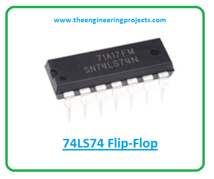
 Hi Friends! Hope you’re well today. I welcome you on board. In this post today, I’ll describe the Introduction to 74LS74.
74LS74A flip-flop IC carries the Schottky TTL circuitry to generate high-speed D-type flip-flops. Every flip-flop in this chip comes with individual inputs, and also complementary Q and Q`(bar) outputs.
Flip-Flops are normally considered as the basic building blocks of modern digital electronics. These flip-flops are used to store the binary data where stored data can be varied by applying the different inputs.
I suggest you buckle up as in this post I’ll walk you through the complete introduction to 74LS74 covering datasheet, pinout, features, and applications.
Let’s get started.
Introduction to 74LS74
- 74LS74A flip-flop IC carries the Schottky TTL circuitry to generate high-speed D-type flip-flops. Every flip-flop in this chip comes with individual inputs, and also complementary Q and Q`(bar) outputs.
- A flip-flop is a circuit that comes with two stable states and is mainly employed to store binary data.
- These flip-flops are widely used in communication systems and computers.
- The working of 74LS74 is simple and straight forward. In order to activate the chip, power the GND and Vcc pin of the chip. In this dual D flip-flop, each flip-flop works independently.
- To achieve the output at pins 5 and 6, you’ll need to use 1st flip-flip by connecting the input signals 2 and 3. The clock source is produced using MCU or 555 timers and is provided to pin 3. When you keep pin 3 HIGH, it will reset the flip-flop and clear the data.
74LS74 Flip-Flop Table
You can get a hold of the working of this chip by observing the table below where X represents ‘don’t care’
74LS74 Datasheet
Before you incorporate this device into your electrical project, it’s wise to go through the datasheet of the component that features the main characteristics of the component. You can download the datasheet of 74LS74 by clicking the link below.
74LS74 Pinout
The following figure represents the pinout diagram of 74LS74.
The following table shows the pin description of each pin incorporated on the chip.
| Pin Description of 74LS74 | ||||
|---|---|---|---|---|
| Pin No. & Name | Description | Symbol | ||
| 5,9 Output | Output Pin of the Flip Flop | 1Q / 2Q | ||
| 6,8 Complementary Output | The inverted output pin of Flip Flop | 1Q’(bar) / 2Q’(bar) | ||
| 3,11 Clock Input Pin | These pins should be provided with a clock pulse for the flip flop | 1CLK / 2CLK | ||
| 1,13 Clear data | Resets the flip flop by clearing its memory | 1CLR (bar) / 2CLR (bar) | ||
| 2,12 Data input pin | Input pin of the Flip Flop | 1D /2D | ||
| 4,10 PRE Input | Another Input pin for Flip Flop. Also referred to as a set pin | 1PRE (bar) / 2PRE (bar) | ||
| 7 Ground | Connected to the ground | Vss | ||
| 14 Supply Voltage | Power Supply | Vdd/Vcc | ||
74LS74 Features
The following are the main features of 74LS74.
- Low-Level Input Voltage maximum = 0.8V
- Operating Voltage range = 2V to 15V
- Operating Temperature range = 0 to 70°C
- Dual D Flip Flop Package IC
- High-Level Output Current = 8mA
- High-Level Input Voltage minimum = 2 V
- Propagation Delay = 40nS
- Available packages = 14-pin SO-14, SOT42
74LS74 Equivalents
The equivalents to 74LS74 are:
- HEF40312B
- 74LVC2G80
74LS74 Applications
- Buffer Circuits
- Latching devices
- Used as Shift Registers
- Sampling Circuits
- Memory/Control Registers
That’s all for today. Hope you find this article helpful. If you’re unsure or have any questions, you can approach me in the section below, I’d love to help you the best way I can. You are most welcome to share your valuable feedback and suggestions around the content we share so we keep coming back with quality content customized to your exact needs and requirements. Thank you for reading the post.
JLCPCB – Prototype 10 PCBs for $2 (For Any Color)
China’s Largest PCB Prototype Enterprise, 600,000+ Customers & 10,000+ Online Orders Daily
How to Get PCB Cash Coupon from JLCPCB: https://bit.ly/2GMCH9w
The post 74LS74 Dual D Flip-Flop Datasheet, Pinout, Features & Applications appeared first on The Engineering Projects.


No comments:
Post a Comment