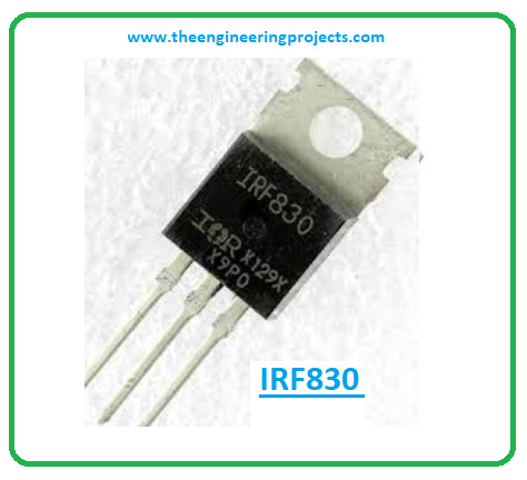
 Hello Guys! Hope you’re well today. I welcome you on board. In this post today, I’ll walk you through the Introduction to IRF830.
The IRF830 is an n-channel power MOSFET where conduction is carried out by both electrons and holes but electrons are the major carriers and holes are the minority carriers. It is a high voltage and fast switching device that comes with low on-state resistance.
You can also check this post on the Introduction to IRF730 that I’ve uploaded previously.
I suggest you buckle up and read this post all the way through as I’ll detail the complete Introduction to IRF830 covering datasheet, pinout, features, equivalent, and applications.
Let’s get started.
Introduction to IRF830
- The IRF830 is an n-channel power MOSFET where electrons are the major carriers and holes are the minority carriers.
- It is widely used in amplification and switching applications of the electrical circuits.
- The MOSFET stands for Metal Oxide Silicon Field Effect Transistor that is produced by the controlled oxidation of a silicon semiconductor material. It is also known as IGFET Insulated Gate Field Effect Transistor.
- This device is an n-channel MOSFET which means the conduction is carried out due to the movement of electrons in opposed to the p-channel MOSFET where the conduction process is carried out by the movement of holes.
- Know that, conduction process is done by both the movement of electrons and holes but in the case of n-channel MOSFET the major carriers are electrons and in the case of p-channel MOSFET major carriers are holes.
- With maximum drain-to-source voltage around 500V, this IRF830 MOSFET is a three-pin component made of gate (G) drain (D), and source (S) terminals. These terminals are used for the external connection with the electrical circuits.
- In terms of the controlled value, the MOSFET is different from the BJT semiconductors. The MOSFETs are voltage-controlled devices while the BJT (bipolar junction transistors) are current-controlled devices.
- These devices, however, are the same in terms of performance and efficiency. Both are high speed and low power loss devices.
- The voltage at the gate pin controls the current between source and drain terminals. The gate terminal behaves like a control value that controls the conduction between source and drain terminals.
- When a voltage signal is applied at the gate terminal, the current starts flowing between the source and drain terminals.
IRF830 Datasheet
Before applying this component to your electrical project, it’s better to go through the datasheet of the component that highlights the main characteristics of the device. You can download the datasheet of this component IRF830 by clicking the link mentioned below.
IRF830 Pinout
The IRF830 is an N-channel power MOSFET that contains three pins named
1: Gate
2: Drain
3: Source
- The gate pin controls the current between the source and drain terminals when we apply a voltage signal on the gate pin
- The following figure shows the pinout diagram of IRF830 MOSFET.
Know that… typically, the MOSFET is a four-pin device that comes with a Source (S), Gate (G), Drain (D), and a Body (B) / Substrate. The bodyside is always connected to the source terminal thus the MOSFET operates as a three-terminal device.
IRF830 Equivalent
The following are the equivalent to IRF830.
- FTK480
- 8N50
- KF12N50
While working with the alternatives, always check the pinout as it’s possible the pinout of the alternatives might differ from the pinout of this device.
IRF830 Features
The following are the main features of IRF830. These features will help you understand how this device is different from its peers available in the market.
- Type = n-channel power MOSFET
- Package = TO-220
- Gate threshold voltage (VGS-th) = 10V (limit = ±20V)
- Continuous Drain Current (ID) = 4.5A
- Drain to Source Breakdown Voltage = 500V
- Rise time is 16nS and fall time is 16nS
- Drain Source Resistance (RDS) = 1.5 Ohms
One main disadvantage of this IRF830 MOSFET is its high on-resistance (RDS) value which stands around 1.5 ohms. Though this device is used for switching applications, it cannot be used in the applications where high switching efficiency is needed… due to its high on-resistance.
IRF830 Applications
The IRF830 is used in the following applications.
- Used in motor control and UPS.
- LED dimmers or flashers.
- Incorporated in high-efficiency DC to DC converters.
- Used in inverter circuits.
- Used in switching and amplifying applications.
That’s all for today. If you have any questions, you can approach me in the section below, I’d love to help you the best way I can. Feel free to keep us updated with your valuable feedback and suggestions around the content we share so we keep producing quality content customized to your exact requirements. Thank you for reading this post.
JLCPCB – Prototype 10 PCBs for $2 (For Any Color)
China’s Largest PCB Prototype Enterprise, 600,000+ Customers & 10,000+ Online Orders Daily
How to Get PCB Cash Coupon from JLCPCB: https://bit.ly/2GMCH9w
The post IRF830 MOSFET Datasheet, Pinout, Features, Equivalent & Applications appeared first on The Engineering Projects.


No comments:
Post a Comment